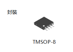
|
S-19630A
Automotive, 125��C Operation, Low Input Offset Voltage CMOS Operational Amplifier S-19630A Describe: This IC incorporates a general purpose analog circuit in a small package. This is a zero-drift operational amplifier with Rail-to-Rail input and output, which uses chopper-stabilizing techniques to provide low input offset voltage. The S-19630AB is a dual operational amplifier (2 circuits), which is suitable for applications requiring less offset voltage.
Features: • Low input offset voltage: VIO = +50 ��V max. (Ta = −40��C to +125��C) • Low input offset voltage drift: ��VIO/��Ta = ��25 nV/��C typ. (VDD = 30.0 V, Ta = −40��C to +125��C) • Operation power supply voltage range: VDD = 4.0 V to 36.0 V • Low current consumption (Per circuit): IDD = 250 ��A typ. • Low input noise voltage: VNOISE_pp = 0.8 ��Vpp typ. (f = 0.1 Hz to 10 Hz) • Low input noise voltage density: VNOISE = 25 nV/��Hz typ. (f = 1 kHz) • Built-in output current limit circuit: Overcurrent limit when output pin is short-circuited • Internal phase compensation: No external parts required • Rail-to-Rail input and output • Operation temperature range: Ta = −40��C to +125��C • Lead-free (Sn 100%), halogen-free • AEC-Q100 qualified*1 *1. Contact our sales representatives for details. Applications: • High-accuracy current detection • Various sensor interfaces • Strain gauge amplifier |

|
S-19611A
Automotive, 105��C Operation, Low Input Offset Voltage CMOS Operational Amplifier S-19611A Describe: This IC incorporates a general purpose analog circuit in a small package. This is a zero-drift operational amplifier with Rail-to-Rail input and output, which uses auto-zeroing techniques to provide low input offset voltage. The S-19611AB is a dual operational amplifier (2 circuits), which is suitable for applications requiring less offset voltage. Features: • Low input offset voltage: VIO = +17 ��V max. (Ta = +25��C) VIO = +100 ��V max. (Ta = −40��C to +105��C) • Operation power supply voltage range: VDD = 2.65 V to 5.50 V • Low current consumption (Per circuit): IDD = 200 ��A typ. • Internal phase compensation: No external parts required • Rail-to-Rail input and output • Operation temperature range: Ta = −40��C to +105��C • Lead-free (Sn 100%), halogen-free • AEC-Q100 qualified*1 *1. Contact our sales representatives for details. Applications: • High-accuracy current detection • Various sensor interfaces • Strain gauge amplifier |


 S19630A_E.pdf