|
S-19914/15 A/B
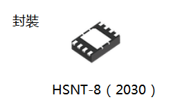
Describe: The S-19914/19915 Series is a step-down switching regulator developed using high withstand voltage CMOS process technologies. This IC has high maximum operation voltage of 36 V and maintains high-accuracy FB pin voltage at ��1.5%. It has a built-in spread spectrum clock generation circuit capable of reducing conductive noise and emission noise during PWM operation. As suitable packages for high-density mounting, such as small-sized HSNT-8(2030), are adopted, this IC contributes to miniaturization of electronic equipment. Since the S-19914/19915 Series has the built-in synchronous circuit, it achieves high efficiency easier compared with conventional step-down switching regulators. In addition, it has the built-in overcurrent protection circuit which protects the IC and coils from excessive load current as well as a thermal shutdown circuit which prevents damage from heat generation. Features:
Applications:
|
|
S-19902A/S-19902B/S-19903A/S-19903B
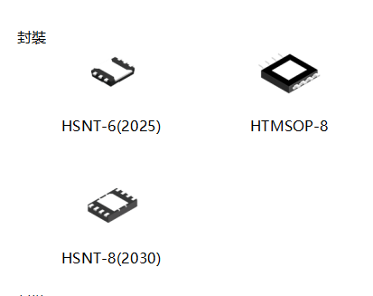
Automotive, 125��C Operation, 36V Input, 600 mA Synchronous Step-Down Switching Regulator S-19902A/19902B/19903A/19903B Series Describe: The S-19902/19903 Series is a step-down switching regulator developed using high withstand voltage CMOS process technologies. This IC has high maximum operation voltage of 36 V and maintains high-accuracy FB pin voltage at ��1.5%. PWM control (S-19902 Series) or PWM / PFM switching control (S-19903 Series) can be selected as an option. Since the S-19902/19903 Series has the built-in synchronous circuit, it achieves high efficiency easier compared with conventional step-down switching regulators. In addition, it has the built-in overcurrent protection circuit which protects the IC and coils from excessive load current as well as a thermal shutdown circuit which prevents damage from heat generation. Features: • Input voltage: 4.0 V to 36.0 V • Output voltage (externally set): 2.5 V to 12.0 V • Output current: 600 mA • FB pin voltage accuracy: ��1.5% • Efficiency: 91% • Oscillation frequency: 2.2 MHz typ. • Overcurrent protection function: 1.2 A typ. (pulse-by-pulse method) • Thermal shutdown function: 170��C typ. (detection temperature) • Short-circuit protection function: Hiccup control, Latch control • 100% duty cycle operation: for home electric appliance • Soft-start function: 5.8 ms typ. • Under voltage lockout function (UVLO): 3.35 V typ. (detection voltage) • Input and output capacitors: Ceramic capacitor compatible • Operation temperature range: Ta = −40��C to +125��C • Lead-free (Sn 100%), halogen-free • Withstand 45 V load dump • AEC-Q100 qualified*1 *1. Contact our sales representatives for details. Applications: • Camera module • For automotive use (engine, transmission, suspension, ABS, related-devices for EV / HEV / PHEV, etc.) • Constant-voltage power supply or electrical application for vehicle interior • Constant-voltage power supply for industrial equipment • Constant-voltage power supply |
|
S-19932A/S-19932B/S-19933A/S-19933B
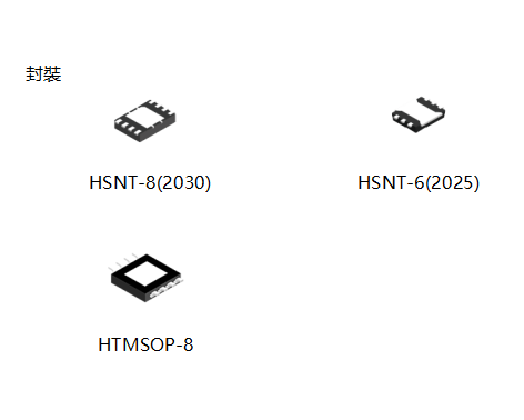
Automotive, 125��C Operation, 18V Input, 600mA Synchronous Step-Down Switching Regulator S-19932A/19932B/19933A/19933B Series Describe: The S-19932/19933 Series is a step-down switching regulator developed using high withstand voltage CMOS process technologies. This IC has high maximum operation voltage of 18 V and maintains high-accuracy FB pin voltage at ��1.5%. PWM control (S-19932 Series) or PWM / PFM switching control (S-19933 Series) can be selected as an option. Since the S-19932/19933 Series has the built-in synchronous circuit, it achieves high efficiency easier compared with conventional step-down switching regulators. In addition, it has the built-in overcurrent protection circuit which protects the IC and coils from excessive load current as well as a thermal shutdown circuit which prevents damage from heat generation. Features: • Input voltage: 4.0 V to 18.0 V • Output voltage (externally set): 1.0 V to 12.0 V • Output current: 600 mA • FB pin voltage accuracy: ��1.5% • Efficiency: 91% • Oscillation frequency: 2.2 MHz typ. • Overcurrent protection function: 1.2 A typ. (pulse-by-pulse method) • Thermal shutdown function: 170��C typ. (detection temperature) • Short-circuit protection function: Hiccup control, Latch control • 100% duty cycle operation: for home electric appliance • Soft-start function: 5.8 ms typ. • Under voltage lockout function (UVLO): 3.35 V typ. (detection voltage) • Input and output capacitors: Ceramic capacitor compatible • Operation temperature range: Ta = −40��C to +125��C • Lead-free (Sn 100%), halogen-free • AEC-Q100 qualified*1 *1. Contact our sales representatives for details. Applications: • Camera module • For automotive use (engine, transmission, suspension, ABS, related-devices for EV / HEV / PHEV, etc.) • Constant-voltage power supply for electrical application for vehicle interior • Constant-voltage power supply for industrial equipment • Constant-voltage power supply |
|
S-19944A/S-19944B/S-19945A/S-19945B
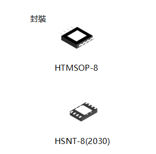
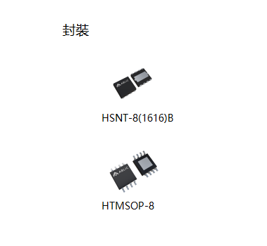
Automotive, 125��C Operation, 18 V Input, 1 A, Low EMI, Synchronous Step-down Switching Regulator S-19944A/19944B/19945A/19945B Series Describe: The S-19944/19945 Series is a step-down switching regulator developed using high withstand voltage CMOS process technologies. This IC has high maximum operation voltage of 18 V and maintains high-accuracy FB pin voltage at ��1.5%. As suitable packages for high-density mounting, such as small-sized HSNT-8(2030), are adopted, this IC contributes to miniaturization of electronic equipment. PWM control (S-19944 Series) or PWM / PFM switching control (S-19945 Series) can be selected as an option. Since the S-19944/19945 Series has the built-in synchronous circuit, it achieves high efficiency easier compared with conventional step-down switching regulators. In addition, it has the built-in overcurrent protection circuit which protects the IC and coils from excessive load current as well as a thermal shutdown circuit which prevents damage from heat generation. Features: • Input voltage: 4.0 V to 18.0 V • Output voltage (externally set): 1.0 V to 12.0 V • Output current: 1 AQ • FB pin voltage accuracy: ��1.5% • Efficiency: 91% • Oscillation frequency: 2.2 MHz typ. • Spread spectrum clock generation function: FSSS = +6% typ. (Diffusion rate) • Overcurrent protection function: 1.85 A typ. (pulse-by-pulse method) • Thermal shutdown function: 170��C typ. (detection temperature) • Short-circuit protection function: Hiccup control, Latch control for home electric appliance • 100% duty cycle operation: • Soft-start function: 5.8 ms typ. • Under voltage lockout function (UVLO): 3.35 V typ. (detection voltage) • Input and output capacitors: Ceramic capacitor compatible • Operation temperature range: Ta = −40��C to +125��C • Lead-free (Sn 100%), halogen-free • AEC-Q100 qualified*1 *1. Contact our sales representatives for details. Applications: • Camera module • For automotive use (engine, transmission, suspension, ABS, related-devices for EV / HEV / PHEV, etc.) • Constant-voltage power supply for electrical application for vehicle interior • Constant-voltage power supply for industrial equipment • Constant-voltage power supply |
|
S-19954/S-19955
Automotive, 125��C Operation, 5.5 V Input, 1 A, Power Good, Synchronous Step-down Switching Regulator S-19954/19955 Series Describes: PWM control (S-19954 Series) or PWM / PFM switching control (S-19955 Series) can be selected as an option. S-19954 Series, which features PWM control, can be used without interfering with AM radio bands. Since the S-19955 Series, which features PWM / PFM switching control, operates with PWM control under heavy load and automatically switches to PFM control under light load. It achieves high-efficiency operation in accordance with the device's status. This IC is implemented as a small package and can comprise an application circuit with a coil and two capacitors at the minimum configuration. Since the switching frequency is as high as 2.25 MHz, and the peripheral parts can be made compact, the IC is suitable for space-saving uses. Features: • Input voltage: 2.7 V to 5.5 V • Output voltage: 0.8 V to 3.3 V equipment • Output current: 1 A • VOUT pin detection voltage accuracy: ��1.5% (Tj = −40��C to +125��C) • Efficiency: 95% • Oscillation frequency: 2.25 MHz typ. • Overcurrent protection function: 1.75 A typ. (pulse-by-pulse method) • Thermal shutdown function: 170��C typ. (detection temperature) • Short-circuit protection function: Hiccup control, Latch control • 100% duty cycle operation • Output discharge function: "Available " / "Unavailable " is selectable. • Power Good function: Nch open-drain output • Soft-start function: 0.35 ms typ. • Under voltage lockout function (UVLO): 2.43 V typ. (detection voltage) • Input and output capacitors: Ceramic capacitor compatible • Operation temperature range: Ta = −40��C to +125��C • Lead-free (Sn 100%), halogen-free • AEC-Q100 in process*1 *1. Contact our sales representatives for details. Applications: • Secondary power supply for automotive • Camera module • For automotive use (engine, transmission, suspension, ABS, related-devices for EV / HEV / PHEV, etc.) • Constant-voltage power supply for electrical application for vehicle interior |
|
S-19212B/DxxA Series
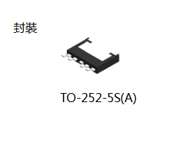
Automotive, 125��C Operation, 36 V Input, 250 mA Voltage Regulator S-19212B/DxxA Series. Describe: The S-19212B/DxxA Series, developed by using high-withstand voltage CMOS process technology, is a positive voltage regulator with a high-withstand voltage, low current consumption and high-accuracy output voltage, and has a built-in ON / OFF circuit. ABLIC Inc. offers FIT rate calculation and Thermal simulation service. Features: • Output voltage: 2.5 V to 16.0 V, selectable in 0.1 V step • Input voltage: 3.0 V to 36 V • Output voltage accuracy: ��2.0% (Tj = −40��C to +125��C) • Current consumption: During operation: 6.5 ��A typ., 8.5 ��A max. (Tj = −40��C to +125��C) During power-off: 0.1 ��A typ., 3.5 ��A max. (Tj = −40��C to +125��C) • Output current: Possible to output 250 mA (at VIN �� VOUT(S) + 2.0 V)*1 • Input capacitor: A ceramic capacitor can be used. (1.0 ��F or more) • Output capacitor: A ceramic capacitor can be used. (1.0 ��F to 100 ��F) • Built-in overcurrent protection circuit: Limits overcurrent of output transistor. • Built-in thermal shutdown circuit: Detection temperature 165��C typ. • Built-in ON / OFF circuit: Ensures long battery life. Discharge shunt function is available. • Operation temperature range: Ta = −40��C to +125��C • Lead-free (Sn 100%), halogen-free • Withstand 45 V load dump • AEC-Q100 qualified*2 Applications: • Constant-voltage power supply for electrical application for vehicle interior • Constant-voltage power supply for home electric appliance • For automotive use (engine, transmission, suspension, ABS, related-devices for EV / HEV / PHEV, etc.) |
|
19246xxxH
Automotive, 105��C Operation, 10 V Input, 2000 mA Voltage Regulator with Soft-start Function S-19246xxxH Series Describe: The S-19246xxxH Series developed by using high-withstand voltage CMOS process technology, is a positive voltage regulator with high-accuracy output voltage and high output current. A built-in overcurrent protection circuit to limit overcurrent of the output transistor and a built-in thermal shutdown circuit to limit heat are included. Also, the S-19246xxxH Series includes the soft-start function to adjust the output voltage rising time at power-on or at the time when the ON / OFF pin is set to ON. Features: • Output voltage: 1.0 V to 6.0 V, selectable in 0.05 V step • Input voltage: 2.5 V to 10.0 V • Output voltage accuracy: ��2.3% (Tj = −40��C to +105��C) • Dropout voltage: 0.62 V typ. (3.0 V output product, at IOUT = 2000 mA) • Current consumption: During operation: 120 ��A typ., 150 ��A max. (Tj = −40��C to +150��C) During power-off: 0.1 ��A typ., 4.5 ��A max. (Tj = −40��C to +105��C) • Output current: Possible to output 2000 mA (at VIN �� VOUT(S) + 1.0 V)*1 • Ripple rejection: 60 dB typ. (at f = 1.0 kHz) • Built-in overcurrent protection circuit: Limits overcurrent of output transistor. • Built-in thermal shutdown circuit: Detection temperature 170��C typ. • Built-in soft-start circuit: Adjusts output voltage rising time at power-on or at the time when ON / OFF pin is set to ON. tSS = 6.0 ms typ. (CSS = 10 nF) Soft-start time can be changed by the capacitor (CSS). • Built-in ON / OFF circuit: Ensures long battery life Discharge shunt function "available" / "unavailable" is selectable. Pull-down function "available" / "unavailable" is selectable. • Operation temperature range: Ta = −40��C to +105��C • Lead-free (Sn 100%), halogen-free • AEC-Q100 qualified*2 *1. Please make sure that the loss of the IC will not exceed the power dissipation when the output current is large. *2. Contact our sales representatives for details. Applications: • Constant-voltage power supply for telecommunication module • Constant-voltage power supply for home electric appliance • For automotive use (car body, headlight, ITS, accessory, car navigation system, car audio system, etc.) |
|
S-19255
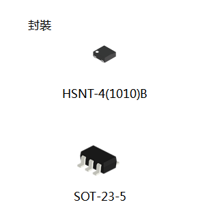
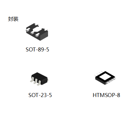
Automotive, 125��C Operation, 5.5 V Input, 300 mA Voltage Regulator S-19255 Series Describe: The S-19255 Series, developed by using CMOS process technology, is a positive voltage regulator with high-accuracy output voltage. This IC has high ripple-rejection of 80 dB typ. Also, a built-in overcurrent protection circuit to limit overcurrent of the output transistor and a built-in thermal shutdown circuit to limit heat are included. In addition to the conventional small package SOT-23-5, the super-small package HSNT-4(1010)B is added to the lineup, which realizes higher-density mounting. Features: • Output voltage: 0.9 V to 3.6 V, selectable in 0.05 V step • Input voltage: 1.5 V to 5.5 V • Output voltage accuracy: ��2.0% (Tj = −40��C to +125��C) • Current consumption: During operation: 55 ��A typ., 89 ��A max. (Tj = −40��C to +125��C) During power-off: 0.1 ��A typ., 6.4 ��A max. (Tj = −40��C to +125��C) • Dropout voltage: 120 mV typ. (HSNT-4(1010)B package products, 2.5 V output product, at IOUT = 200 mA) • Output current: Possible to output 300 mA (at VIN �� VOUT(S) + 1.0 V)*1 • Ripple rejection: 50 dB typ. (VOUT(S) = 3.3 V, at f = 100 kHz) 80 dB typ. (VOUT(S) = 3.3 V, at f = 1.0 kHz) • Input capacitor: A ceramic capacitor can be used. (0.1 ��F or more) • Output capacitor: A ceramic capacitor can be used. (1.0 ��F or more) • Built-in overcurrent protection circuit: Limits overcurrent of output transistor. • Built-in thermal shutdown circuit: Detection temperature 175��C typ. • Built-in ON / OFF circuit: Ensures long battery life. Pull-down function "available" / "unavailable" is selectable. Discharge shunt function "available" / "unavailable" is selectable. • Operation temperature range: Ta = −40��C to +125��C • Lead-free (Sn 100%), halogen-free • AEC-Q100 qualified*2 *1. Please make sure that the loss of the IC will not exceed the power dissipation when the output current is large. *2. Contact our sales representatives for details. Applications: • For automotive use (engine, transmission, suspension, ABS, related-devices for EV / HEV / PHEV, etc.) • For automotive use (front sensing camera, DMS, FCW): SOT-23-5 package product • For automotive use (accessory, car navigation system, car audio system, etc.) • Surround view camera for automotive: HSNT-4(1010)B package product • Constant-voltage power supply for electrical application for vehicle interior |
|
S-19310
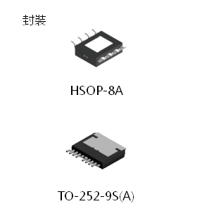
Automotive, 125��C Operation, 36 V Input, 40 mA Voltage Regulator with Reset Function S-19310 Series Describe: The S-19310 Series, developed by using high-withstand voltage CMOS process technology, is a positive voltage regulator with the reset function, which has high-withstand voltage and low current consumption. Regarding a release signal output in the reset function, the S-19310 Series enables delay time adjustment by an external capacitor. Output form of the reset function is selectable from Nch open-drain output or CMOS output. Features: Regulator block • Output voltage: 2.9 V to 5.3 V, selectable in 0.1 V step • Input voltage: 3.0 V to 36.0 V • Output voltage accuracy: ��2.0% (Tj = −40��C to +125��C) • Dropout voltage: 240 mV typ. (VOUT(S) = 5.0 V, IOUT = 30 mA) • Output current: Possible to output 40 mA (VIN = VOUT(S) + 2.0 V)*1 • Input and output capacitors: A ceramic capacitor can be used. (1.0 ��F or more) • Built-in overcurrent protection circuit: Limits overcurrent of output transistor • Built-in thermal shutdown circuit: Detection temperature 160��C typ. Detector block • Detection voltage: 2.6 V to VOUT(S) − 0.3 V, selectable in 0.1 V step • Operation voltage: A type: 1.8 V to 36.0 V B type: 2.5 V to 36.0 V • Detection voltage accuracy: ��2.0% (Tj = −40��C to +125��C) • Hysteresis width selectable from "Available" / "Unavailable": "Available": 5.0% �� VHYS �� 30.0% (Tj = −40��C to +125��C) "Unavailable": VHYS = 0% • Release delay time accuracy: ��20% (CD = 3.3 nF, Tj = −40��C to +125��C) • Output form: Nch open-drain output CMOS output Overall • Current consumption: 2.2 ��A typ. (Tj = −40��C to +125��C) • Operation temperature range: Ta = −40��C to +125��C • Lead-free (Sn 100%), halogen-free • Withstand 45 V load dump • AEC-Q100 qualified*2 *1. Please make sure that the loss of the IC will not exceed the power dissipation when the output current is large. *2. Contact our sales representatives for details. Applications: • Constant-voltage power supply and reset circuit for automotive electric component • Power supply and reset circuit for low-current battery-powered device |
|
S-19213
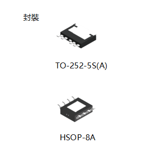
Automotive, 125��C Operation, 36 V Input, 1000 mA Voltage Regulator S-19214 Series Describe: The S-19214 Series developed by using high-withstand voltage CMOS process technology, is a positive voltage regulator with a high-withstand voltage, low current consumption and high-accuracy output voltage. The S-19214 Series operates at the maximum operation voltage of 36 V and a low current consumption of 5.0 ��A typ. and has a built-in low on-resistance output transistor, which provides a very small dropout voltage and a large output current. In addition to the type in which output voltage is set inside the IC, the type for which output voltage can be set via an external resistor is added to a lineup. Also, a built-in overcurrent protection circuit to limit overcurrent of the output transistor and a built-in thermal shutdown circuit to limit heat are included. Features: • Output voltage (internally set): 1.8 V, 3.0 V, 3.3 V, 5.0 V, 8.0 V, 12.0 V • Output voltage (externally set): 1.8 V to 30.0 V, settable via external resistor • Input voltage: 2.8 V to 36.0 V • Output voltage accuracy: ��1.5% (Tj = −40��C to +125��C) • Current consumption: During operation: 5.0 ��A typ., 9.8 ��A max. (Tj = −40��C to +125��C) During power-off: 0.1 ��A typ., 2.0 ��A max. (Tj = −40��C to +125��C) • Output current: Possible to output 500 mA (at VIN �� VOUT(S) + 1.0 V)*1 • Input and output capacitors: A ceramic capacitor can be used. (1.0 ��F or more) • Built-in overcurrent protection circuit: Limits overcurrent of output transistor. (with a detection function of the difference between input and output voltage) • Built-in thermal shutdown circuit: Detection temperature 170��C typ. • Built-in ON / OFF circuit: Ensures long battery life. Discharge shunt function is available. Pull-down function is available. • Operation temperature range: Ta = −40��C to +125��C • Lead-free (Sn 100%), halogen-free • Withstand 45 V load dump • AEC-Q100 qualified*2 *1. Please make sure that the loss of the IC will not exceed the power dissipation when the output current is large. *2. Contact our sales representatives for details. Applications: • Constant-voltage power supply for electrical application for vehicle interior • Constant-voltage power supply for home electric appliance • For automotive use (engine, transmission, suspension, ABS, related-devices for EV / HEV / PHEV, etc.) |
|
S-19214
Automotive, 125��C Operation, 36 V Input, 1000 mA Voltage Regulator S-19214 Series Describe: The S-19214 Series developed by using high-withstand voltage CMOS process technology, is a positive voltage regulator with a high-withstand voltage, low current consumption and high-accuracy output voltage. The S-19214 Series operates at the maximum operation voltage of 36 V and a low current consumption of 5.0 ��A typ. and has a built-in low on-resistance output transistor, which provides a very small dropout voltage and a large output current. In addition to the type in which output voltage is set inside the IC, the type for which output voltage can be set via an external resistor is added to a lineup. Also, a built-in overcurrent protection circuit to limit overcurrent of the output transistor and a built-in thermal shutdown circuit to limit heat are included. Features: • Output voltage (internally set): 1.8 V, 3.0 V, 3.3 V, 5.0 V, 8.0 V, 12.0 V • Output voltage (externally set): 1.8 V to 30.0 V, settable via external resistor • Input voltage: 2.8 V to 36.0 V • Output voltage accuracy: ��1.5% (Tj = −40��C to +125��C) • Current consumption: During operation: 5.0 ��A typ., 9.8 ��A max. (Tj = −40��C to +125��C) During power-off: 0.1 ��A typ., 2.0 ��A max. (Tj = −40��C to +125��C) • Output current: Possible to output 1000 mA (at VIN��VOUT(S) + 2.0 V)*1 • Input and output capacitors: A ceramic capacitor can be used. (1.0 ��F or more) • Built-in overcurrent protection circuit: Limits overcurrent of output transistor. (with a detection function of the difference between input and output voltage) • Built-in thermal shutdown circuit: Detection temperature 170��C typ. • Built-in ON / OFF circuit: Ensures long battery life. Discharge shunt function is available. Pull-down function is available. • Operation temperature range: Ta = −40��C to +125��C • Lead-free (Sn 100%), halogen-free • Withstand 45 V load dump • AEC-Q100 qualified*2 *1. Please make sure that the loss of the IC will not exceed the power dissipation when the output current is large. *2. Contact our sales representatives for details. Applications: • Constant-voltage power supply for electrical application for vehicle interior • Constant-voltage power supply for home electric appliance • For automotive use (engine, transmission, suspension, ABS, related-devices for EV / HEV / PHEV, etc.) |
|
S-19251
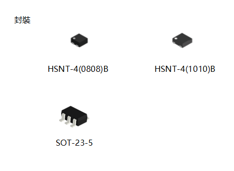
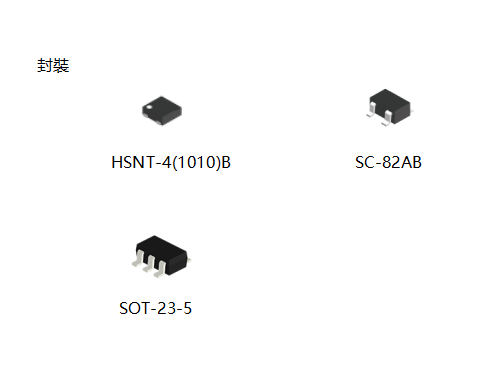
Automotive, 105��c Operation, 5.5 V Input, 150 mA Voltage Regulator S-19251 Series Describe: The S-19251 Series, developed by using CMOS process technology, is a positive voltage regulator with a low current consumption, high ripple-rejection and high-accuracy output voltage. This IC has high ripple-rejection of 75 dB typ., and operates with low current consumption of 20 ��A typ. Also, a built-in overcurrent protection circuit to limit overcurrent of the output transistor and a built-in thermal shutdown circuit to limit heat are included. In addition to the conventional package SOT-23-5, the super-small packages HSNT-4(1010)B and HSNT-4(0808)B are added to the lineup, which realizes higher-density mounting. Features: • Output voltage: 1.0 V to 3.5 V, selectable in 0.05 V step • Input voltage: 1.5 V to 5.5 V • Output voltage accuracy: ��2.5% (Tj = −40��C to +105��C) • Current consumption: During operation: 20 ��A typ., 50 ��A max. (Tj = −40��C to +105��C) During power-off: 0.1 ��A typ., 4.5 ��A max. (Tj = −40��C to +105��C) • Dropout voltage: 0.16 V typ. (2.8 V output product, IOUT = 100 mA) • Output current: Possible to output 150 mA ��VIN��VOUT(S) + 1.0 V)*1 • Ripple rejection: 75 dB typ. (1.2 V output product, f = 1.0 kHz) 70 dB typ. (2.8 V output product, f = 1.0 kHz) • Input capacitor: A ceramic capacitor can be used. (1.0 ��F or more) • Output capacitor: A ceramic capacitor can be used. (1.0 ��F or more) • Built-in overcurrent protection circuit: Limits overcurrent of output transistor. • Built-in thermal shutdown circuit: Detection temperature 150��C typ. • Built-in ON / OFF circuit: Ensures long battery life. Discharge shunt function "available" / "unavailable" is selectable. Pull-down function "available" / "unavailable" is selectable. • Operation temperature range: Ta = −40��C to +105��C • Lead-free (Sn 100%), halogen-free • AEC-Q100 qualified*2 *1. Please make sure that the loss of the IC will not exceed the power dissipation when the output current is large. *2. Contact our sales representatives for details. Applications: • For automotive use (meter, car body, headlight, ITS, accessory, car navigation system, car audio system, etc.) : SOT-23-5 package product • For automotive use (accessory, car navigation system, car audio system, etc.) : HSNT-4(1010)B package product, HSNT-4(0808)B package product |
|
S-19252
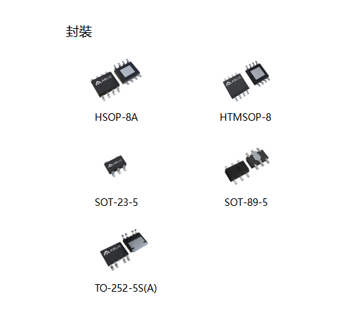
Automotive, 105��C Operation, 5.5 V Input, 150 mA Voltage Regulator with Soft-start Function S-19252 Series Describe: The S-19252 Series, developed by using CMOS process technology, is a positive voltage regulator with high-accuracy output voltage which incorporates the soft-start function. This IC has high ripple-rejection of 80 dB typ., and operates with low current consumption of 36 ��A typ. The S-19252 Series incorporates the soft-start function to adjust the rising time of output voltage immediately after power-on or after the ON / OFF pin is set to ON. It also has a built-in overcurrent protection circuit to limit overcurrent of output transistor. In addition to the conventional small packages SOT-23-5 and SC-82AB, the super-small package HSNT-4(1010)B is added to the lineup, which realizes higher-density mounting. Features: • Output voltage: 1.0 V to 3.6 V, selectable in 0.05 V step • Input voltage: 1.5 V to 5.5 V • Output voltage accuracy: ��15 mV (1.0 V��VOUT(S)��1.5 V��Ta = +25��C) ��1.0% (1.5 V��VOUT(S)��3.6 V��Ta = +25��C) ��3.0% (1.0 V��VOUT(S)��3.6 V��Tj = −40��C ~ +105��C) • Current consumption: During operation: 36 ��A typ., 57 ��A max. (Tj = −40��C to +105��C) During power-off: 0.1 ��A typ., 4.2 ��A max. (Tj = −40��C to +105��C) • Dropout voltage: 70 mV typ. (2.8 V output product, at IOUT = 100 mA) • Output current: Possible to output 150 mA (at VIN �� VOUT(S) + 1.0 V)*1 • Ripple rejection: 70 dB typ. (VOUT(S) �� 2.5 V, at f = 10 kHz) 80 dB typ. (at f = 1.0 kHz) • Input capacitor: A ceramic capacitor can be used. (1.0 ��F or more) • Output capacitor: A ceramic capacitor can be used. (1.0 ��F or more) • Built-in soft-start circuit: The rising time of output voltage immediately after power-on or after the ON/OFF pin is set to ON is adjustable. The soft-start time of SOT-23-5 can be switched to tSS0 = 0.1 ms typ. / tSS1 = 1.0 ms typ. with the SST pin. The soft-start time of SC-82AB is fixed to tSS0 = 0.1 ms typ. The soft-start time of HSNT-4(1010)B is fixed to either tSS0 = 0.1 ms typ. or tSS1 = 1.0 ms typ. • Built-in overcurrent protection circuit: Limits overcurrent of output transistor. • Built-in ON / OFF circuit: Ensures long battery life. Discharge shunt function "available" / "unavailable" is selectable. Pull-down function "available" / "unavailable" is selectable. • Operation temperature range: Ta = −40��C to +105��C • Lead-free (Sn 100%), halogen-free • AEC-Q100 qualified*2 *1. Please make sure that the loss of the IC will not exceed the power dissipation when the output current is large. *2. Contact our sales representatives for details. Applications: • For automotive use (meter, car body, headlight, ITS, accessory, car navigation system, car audio system, etc.) : SOT-23-5 package product, SC-82AB package product • For automotive use (accessory, car navigation system, car audio system, etc.) : HSNT-4(1010)B package product |
|
S-19222
Automotive, 125��C Operation, 36 V Input, 300 mA, Fast Transient Response, Voltage Regulator S-19222xxxA Series Describes: This IC developed by using high-withstand voltage CMOS process technology, is a positive voltage regulator with ahigh-withstand voltage, low current consumption and high-accuracy output voltage. This IC operates at the maximum operation voltage of 36 V and has a built-in low on-resistance output transistor, which provides a very small dropout voltage and a large output current. In addition, favorable transient response characteristics ensure stable output voltage even if the power supply voltage should be impacted by transient fluctuations. The regulator can be combined with a 0.1 ��F low-capacity input capacitor. Features: • Output voltage (internally set): 1.8V, 2.5V, 3.0V, 3.3V, 5.0V, 5.5V, 6.0V • Output voltage (externally set): 1.8 V to 30.0 V, settable via external resistor • Input voltage: 3.0 V to 36.0 V • Output voltage accuracy: ��1.5% (Tj=−40��C to +125��C) • Current consumption: During operation: 22.0 ��A typ., 40.0 ��A max. (Tj=−40��C to +125��C) During power-off: 0.1 ��A typ., 0.5 ��A max. (Tj=−40��C to +125��C) • Output current: Possible to output 300 mA (at VIN �� VOUT(S) + 2.0 V)*1 • Ripple rejection: 75 dB typ. (at f=1.0 kHz) • Input capacitor: A ceramic capacitor can be used. (0.1 ��F or more) • Output capacitor: A ceramic capacitor can be used. (1.0 ��F or more) • Fast transient response: • Built-in overcurrent protection circuit: Limits overcurrent of output transistor. • Built-in thermal shutdown circuit: Detection temperature 170��C typ. • Built-in ON / OFF circuit: Ensures long battery life. Discharge shunt function is available. Pull-down function is available. • Operation temperature range: Ta = −40��C to +125��C • Lead-free (Sn 100%), halogen-free • Withstand 45 V load dump • AEC-Q100 in process*2 *1. Please make sure that the loss of the IC will not exceed the power dissipation when the output current is large. *2. Contact our sales representatives for details. Applications: • Constant-voltage power supply for electrical application for vehicle interior • Constant-voltage power supply for home electric appliance • For automotive use (engine, transmission, suspension, ABS, related-devices for EV / HEV / PHEV, etc.) |

|
S-19243xxxxA
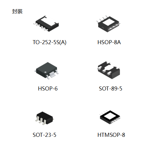
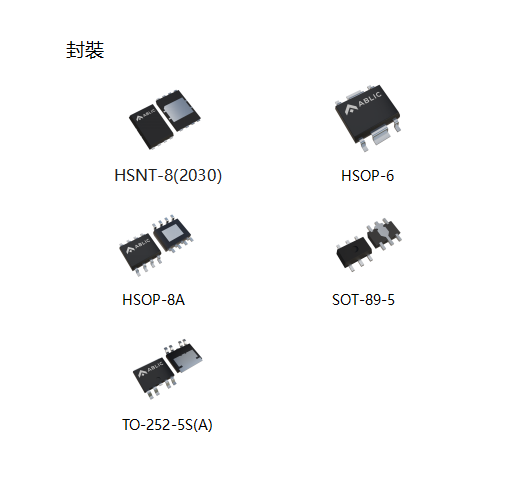
Automotive, 125��C Operation, 10 V Input, 500 mA Voltage Regulator with Soft-start Function S-19243xxxA Series Describes: The S-19243xxxA Series developed by using high-withstand voltage CMOS process technology, is a positive voltage regulator with high-accuracy output voltage and high output current. A built-in overcurrent protection circuit to limit overcurrent of the output transistor and a built-in thermal shutdown circuit to limit heat are included. In addition to the type in which output voltage is set inside the IC, the type for which output voltage can be set via an external resistor is added to a lineup. Features: • Output voltage (internally set): 0.9 V to 6.0 V, selectable in 0.05 V step • Output voltage (externally set): 1.0 V to 9.0 V, settable via external resistor (HSOP-8A, HSOP-6 and HSNT-8(2030) only) • Input voltage: 2.5 V to 10.0 V • Output voltage accuracy: ��2.3% (Tj = −40��C to +125��C) • Dropout voltage: 0.09 V typ. (2.6 V output product, at IOUT = 200 mA) • Current consumption: During operation: 120 ��A typ., 150 ��A max. (Tj = −40��C to +150��C) During power-off: 0.1 ��A typ., 10.5 ��A max. (Tj = −40��C to +125��C) • Output current: Possible to output 500 mA (at VIN �� VOUT(S) + 1.0 V)*1 • Ripple rejection: 60 dB typ. (at f = 1.0 kHz) • Built-in overcurrent protection circuit: Limits overcurrent of output transistor. • Built-in thermal shutdown circuit: Detection temperature 170��C typ. • Built-in soft-start circuit: Adjusts output voltage rising time at power-on or at the time when ON / OFF pin is set to ON. Adjustable type: E / F / G / H type, tSS = 6.0 ms typ. (CSS = 10 nF) Soft-start time can be changed by the capacitor (CSS). Fixed type: A / B / C / D type: Fixed to tSS = 1.0 ms typ. • Built-in ON / OFF circuit: Ensures long battery life Discharge shunt function "available" / "unavailable" is selectable. Pull-down function "available" / "unavailable" is selectable. • Operation temperature range: Ta = −40��C to +125��C • Lead-free (Sn 100%), halogen-free • AEC-Q100 qualified*2 *1. Please make sure that the loss of the IC will not exceed the power dissipation when the output current is large. *2. Contact our sales representatives for details. Applications: • Constant-voltage power supply for electrical application for vehicle interior • Constant-voltage power supply for home electric appliance • For automotive use (engine, transmission, suspension, ABS, related-devices for EV / HEV / PHEV, etc.) |
|
S-19243xxxH
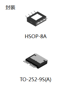
Automotive, 105��C Operation, 10 V Input, 500 mA Voltage Regulator with Soft-start Function S-19243xxxH Series Describes: The S-19243xxxH Series developed by using high-withstand voltage CMOS process technology, is a positive voltage regulator with high-accuracy output voltage and high output current. A built-in overcurrent protection circuit to limit overcurrent of the output transistor and a built-in thermal shutdown circuit to limit heat are included. In addition to the type in which output voltage is set inside the IC, the type for which output voltage can be set via an external resistor is added to a lineup. Features: • Output voltage (internally set): 0.9 V to 6.0 V, selectable in 0.05 V step • Output voltage (externally set): 1.0 V to 9.0 V, settable via external resistor(HSOP-8A, HSOP-6 and HSNT-8(2030) only) • Input voltage: 2.5 V to 10.0 V • Output voltage accuracy: ��2.3% (Tj = −40��C to +105��C) • Dropout voltage: 0.09 V typ. (2.6 V output product, at IOUT = 200 mA) • Current consumption: During operation: 120 ��A typ., 150 ��A max. (Tj = −40��C to +150��C) During power-off: 0.1 ��A typ., 4.5 ��A max. (Tj = −40��C to +105��C) • Output current: Possible to output 500 mA (at VIN �� VOUT(S) + 1.0 V)*1 • Ripple rejection: 60 dB typ. (at f = 1.0 kHz) • Built-in overcurrent protection circuit: Limits overcurrent of output transistor. • Built-in thermal shutdown circuit: Detection temperature 170��C typ. • Built-in soft-start circuit: Adjusts output voltage rising time at power-on or at the time when ON / OFF pin is set to ON. Adjustable type: E / F / G / H type, tSS = 6.0 ms typ. (CSS = 10 nF) Soft-start time can be changed by the capacitor (CSS). Fixed type: A / B / C / D type: Fixed to tSS = 1.0 ms typ. • Built-in ON / OFF circuit: Ensures long battery life Discharge shunt function "available" / "unavailable" is selectable. Pull-down function "available" / "unavailable" is selectable. • Operation temperature range: Ta = −40��C to +105��C • Lead-free (Sn 100%), halogen-free • AEC-Q100 qualified*2 *1. Please make sure that the loss of the IC will not exceed the power dissipation when the output current is large. *2. Contact our sales representatives for details. Applications: • Constant-voltage power supply for electrical application for vehicle interior • Constant-voltage power supply for home electric appliance • For automotive use (car body, headlight, ITS, accessory, car navigation system, car audio system, etc.) |
|
S-19514/S-19515
Automotive, 125��C Operation, 36 V Input, 250 mA, Built-in Window Watchdog Timer, Voltage Regulator with Reset Function S-19514/19515 Series Describe: The S-19514/19515 Series, developed by using high-withstand voltage CMOS technology, is a low dropout positive voltage regulator with the window watchdog timer and the reset function, which has high-withstand voltage. The monitoring time of watchdog timer can be adjusted by an external capacitor. Moreover, a voltage detection circuit which monitors the output voltage is also prepared. Features: Regulator block • Output voltage: 3.3 V, 5.0 V • Input voltage: 3.0 V to 36.0 V • Output voltage accuracy: ��2.0% (Tj = −40��C to +150��C) • Dropout voltage: 100 mV typ. (5.0 V output product, IOUT = 100 mA) • Output current: Possible to output 250 mA (VIN = VOUT(S) + 1.0 V)*1 • Input and output capacitors: A ceramic capacitor of 1.0 ��F or more can be used. • Built-in overcurrent protection circuit: Limits overcurrent of output transistor. • Built-in thermal shutdown circuit: Detection temperature 170��C typ. Detector block • Detection voltage: 2.6 V to 4.7 V, selectable in 0.1 V step • Detection voltage accuracy: ��2.0% (Tj = −40��C to +150��C) • Hysteresis width: 0.12 V min. • Release delay time is adjustable*2: 20 ms typ. (CDLY = 10 nF) Watchdog timer block • Watchdog activation current is adjustable: 1.5 mA typ. (WADJ pin is open) • Watchdog trigger time is adjustable*2: 46 ms typ. (CDLY = 10 nF) • Product type is selectable: S-19514 Series (Product with WEN pin (Output: WO / RO pin)) S-19515 Series (Product without WEN pin (Output: WO pin and RO pin)) • Autonomous watchdog operation function: Watchdog timer operates due to detection of load current. • Watchdog mode: Window mode Overall • Current consumption: 3.0 ��A typ. (During watchdog timer deactivation) 5.0 ��A typ. (During watchdog timer activation) • Operation temperature range: Ta = −40��C to +125��C • Lead-free (Sn 100%), halogen-free • Withstand 45 V load dump • AEC-Q100 qualified*3 Applications: • Constant-voltage power supply for automotive electric component, monitoring of microcontroller |

|
S-19516/S-19517
Automotive, 125��C Operation, 36 V Input, 500 mA, Built-in Window Watchdog Timer, Voltage Regulator with Reset Function S-19516/S-19517 Series Describe: The S-19516/19517 Series, developed by using high-withstand voltage CMOS technology, is a low dropout positive voltage regulator with the window watchdog timer and the reset function, which has high-withstand voltage. The monitoring time of watchdog timer can be adjusted by an external capacitor. Moreover, a voltage detection circuit which monitors the output voltage is also prepared. Features: Regulator block • Output voltage: 3.3 V, 5.0 V • Input voltage: 3.0 V to 36.0 V • Output voltage accuracy: ��2.0% (Tj = −40��C to +150��C) • Dropout voltage: 100 mV typ. (5.0 V output product, IOUT = 100 mA) • Output current: Possible to output 500 mA (VIN = VOUT(S) + 1.0 V)*1 • Input and output capacitors: A ceramic capacitor of 1.0 ��F or more can be used. • Built-in overcurrent protection circuit: Limits overcurrent of output transistor. • Built-in thermal shutdown circuit: Detection temperature 170��C typ. Detector block • Detection voltage: 2.6 V to 4.7 V, selectable in 0.1 V step • Detection voltage accuracy: ��2.0% (Tj = −40��C to +150��C) • Hysteresis width: 0.12 V min. • Release delay time is adjustable*2: 20 ms typ. (CDLY = 10 nF) Watchdog timer block • Watchdog activation current is adjustable: 1.5 mA typ. (WADJ pin is open) • Watchdog trigger time is adjustable*2: 46 ms typ. (CDLY = 10 nF) • Product type is selectable: S-19516 Series (Product with WEN pin (Output: WO / RO pin)) S-19517 Series (Product without WEN pin (Output: WO pin and RO pin)) • Autonomous watchdog operation function: Watchdog timer operates due to detection of load current. • Watchdog mode: Window mode Overall • Current consumption: 3.0 ��A typ. (During watchdog timer deactivation) 5.0 ��A typ. (During watchdog timer activation) • Operation temperature range: Ta = −40��C to +125��C • Lead-free (Sn 100%), halogen-free • Withstand 45 V load dump • AEC-Q100 qualified*3 Applications: • Constant-voltage power supply for automotive electric component, monitoring of microcontroller |

|
S-19518
Automotive, 125��C Operation, 36 V Input, 250 mA, Built-in Window Watchdog Timer, Voltage Regulator with Reset Function S-19518 Series. Describe: The S-19518 Series, developed by using high-withstand voltage CMOS technology, is a low dropout positive voltage regulator with the window watchdog timer and the reset function, which has high-withstand voltage. The monitoring time of watchdog timer can be adjusted by an external capacitor. Moreover, a voltage detection circuit which monitors the output voltage is also prepared. eatures Regulator block • Output voltage: 3.3 V, 5.0 V • Input voltage: 3.0 V to 36.0 V • Output voltage accuracy: ��2.0% (Tj = −40��C to +150��C) • Dropout voltage: 100 mV typ. (5.0 V output product, IOUT = 100 mA) • Output current: Possible to output 250 mA (VIN = VOUT(S) + 1.0 V)*1 • Input and output capacitors: A ceramic capacitor of 1.0 ��F or more can be used. • Built-in overcurrent protection circuit: Limits overcurrent of output transistor. • Built-in thermal shutdown circuit: Detection temperature 170��C typ. • Built-in ON / OFF circuit: Ensures long battery life. Detector block • Detection voltage: 2.6 V to 4.7 V, selectable in 0.1 V step • Detection voltage accuracy: ��2.0% (Tj = −40��C to +150��C) • Hysteresis width: 0.12 V min. • Release delay time is adjustable*2: 20 ms typ. (CDLY = 10 nF) Watchdog timer block • Watchdog activation current: 1.5 mA typ. • Watchdog trigger time is adjustable*2: 46 ms typ. (CDLY = 10 nF) • Autonomous watchdog operation function: Watchdog timer operates due to detection of load current. • Watchdog mode: Window mode Overall • Current consumption: 3.2 ��A typ. (During regulator operation, during watchdog timer deactivation) 0.1 ��A typ. (During regulator stop) • Operation temperature range: Ta = −40��C to +125��C • Lead-free (Sn 100%), halogen-free • Withstand 45 V load dump • AEC-Q100 qualified*3 Applications: • Constant-voltage power supply for automotive electric component, monitoring of microcontroller. |
|
S-19519
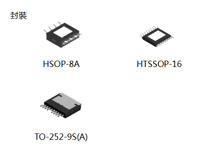
Automotive, 125��C Operation, 36 V Input, 500 mA, Built-in Window Watchdog Timer, Voltage Regulator with Reset Function S-19519 Series. Describe: The S-19519 Series, developed by using high-withstand voltage CMOS technology, is a low dropout positive voltage regulator with the window watchdog timer and the reset function, which has high-withstand voltage. The monitoring time of watchdog timer can be adjusted by an external capacitor. Moreover, a voltage detection circuit which monitors the output voltage is also prepared. Features Regulator block • Output voltage: 3.3 V, 5.0 V • Input voltage: 3.0 V to 36.0 V • Output voltage accuracy: ��2.0% (Tj = −40��C to +150��C) • Dropout voltage: 100 mV typ. (5.0 V output product, IOUT = 100 mA) • Output current: Possible to output 500 mA (VIN = VOUT(S) + 1.0 V)*1 • Input and output capacitors: A ceramic capacitor of 1.0 ��F or more can be used. • Built-in overcurrent protection circuit: Limits overcurrent of output transistor. • Built-in thermal shutdown circuit: Detection temperature 170��C typ. • Built-in ON / OFF circuit: Ensures long battery life. Detector block • Detection voltage: 2.6 V to 4.7 V, selectable in 0.1 V step • Detection voltage accuracy: ��2.0% (Tj = −40��C to +150��C) • Hysteresis width: 0.12 V min. • Release delay time is adjustable*2: 20 ms typ. (CDLY = 10 nF) Watchdog timer block • Watchdog activation current: 1.5 mA typ. (WADJ pin is open) • Watchdog trigger time is adjustable*2: 46 ms typ. (CDLY = 10 nF) • Product type is selectable: S-19519A Series(TO-252-9S package product, HSOP-8A package product) S-19519B Series (HTSSOP-16 package product) • Autonomous watchdog operation function: Watchdog timer operates due to detection of load current. • Watchdog mode: Window mode Overall • Current consumption: 3.2 ��A typ. (During regulator operation, during watchdog timer deactivation) 0.1 ��A typ. (During regulator stop) • Operation temperature range: Ta = −40��C to +125��C • Lead-free (Sn 100%), halogen-free • Withstand 45 V load dump • AEC-Q100 qualified*3 Applications: • Constant-voltage power supply for automotive electric component, monitoring of microcontroller |
|
S-19400/S-19401
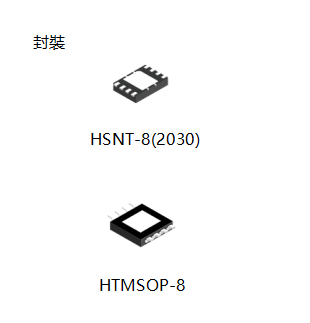
Automotive, 125��C Operation, 3.8 ��A Current Consumption Watchdog Timer with Reset Function S-19400/19401 Series Describe: The S-19400/19401 Series is a watchdog timer developed using CMOS technology, which can operate with low current consumption of 3.8 ��A typ. The reset function and the low voltage detection function are available. Features: • Detection voltage: 2.0 V to 5.0 V, selectable in 0.1 V step • Detection voltage accuracy: ��2.0% • Input voltage: VDD = 0.9 V to 6.0 V • Hysteresis width: 5% typ. • Current consumption during watchdog timer operation: 3.8 ��A typ. • Reset time-out period: 14.5 ms typ. (CPOR = 2200 pF) • Watchdog time-out period: 24.6 ms typ. (CWDT = 470 pF) • Watchdog operation is switchable: Enable, Disable • Watchdog operation voltage range: VDD = 2.5 V to 6.0 V • Watchdog mode switching function*1: Time-out mode, window mode • Watchdog input edge is selectable: Rising edge, falling edge, both rising and falling edges • Product type is selectable: S-19400 Series (Product with W / T pin (Output: WDO pin)) S-19401 Series (Product without W / T pin (Output: RST pin, WDO pin)) • Operation temperature range: Ta = −40��C to +125��C • Lead-free (Sn 100%), halogen-free • AEC-Q100 qualified*2 *1. The S-19401 Series is fixed to the window mode. *2. Contact our sales representatives for details. Applications: • For automotive use (engine, transmission, suspension, ABS, related-devices for EV / HEV / PHEV, etc.) |
|
S-19113xxxA
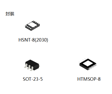
Automotive, 125��C Operation, 36 V, Voltage Detector with SENSE Pin Reverse Connection Protection, Delay Function (External Delay Time Setting) S-19113xxxA Series Describe: This IC, developed using CMOS technology, is a high-accuracy voltage detector. The detection voltage and release voltage are fixed internally with an accuracy of ��1.5%. Apart from the power supply pin, the detection voltage input pin (SENSE pin) is also prepared, so the output is stable even if the SENSE pin voltage (VSENSE) falls to 0 V. The SENSE pin also has a built-in reverse connection protection circuit that reduces current in the SENSE pin during a reverse connection. The release signal can be delayed by setting a capacitor externally, and the release delay time accuracy is ��15% (CD = 3.3 nF). The output form is Nch open-drain output. Features: • Detection voltage: 4.0 V to 10.0 V (0.05 V step) • Detection voltage accuracy: ��1.5% • Hysteresis width selectable from "Available" / "Unavailable": "Available": 5.0%, 10.0% "Unavailable": 0% • Release delay time accuracy: ��15% (CD = 3.3 nF) • Current consumption: 0.6 ��A typ. • Output form: Nch open-drain output • Built-in reverse connection protection circuit: Reduces current in the SENSE pin during a reverse connection. • Operation voltage range: 3.0 V to 36.0 V • Operation temperature range: Ta = −40��C to +125��C • Lead-free (Sn 100%), halogen-free • Withstand 45 V load dump • AEC-Q100 qualified*1 Applications: • Automotive battery voltage detection • For automotive use (engine, transmission, suspension, ABS, related-devices for EV / HEV / PHEV, etc.) |
|
S-19115xxxA
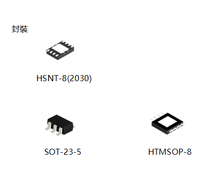
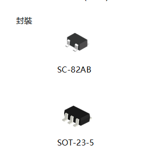
Automotive, 125��C Operation, 36 V, Voltage Detector for Overvoltage Detection with Delay Function (External Delay Time Setting) S-19115xxxA Series Describe: This IC, developed using CMOS technology, is a high-accuracy voltage detector. The detection voltage and release voltage are fixed internally with an accuracy of ��1.5%. Apart from the power supply pin, the detection voltage input pin (SENSE pin) is also prepared, so the output is stable even if the SENSE pin voltage (VSENSE) falls to 0 V. The SENSE pin also has a built-in reverse connection protection circuit that reduces current in the SENSE pin during a reverse connection. The release signal can be delayed by setting a capacitor externally, and the release delay time accuracy is ��15% (CD= 3.3 nF). The output form is Nch open-drain output. Features: • Detection voltage: 16.0 V to 18.0 V (0.1 V step) • Detection voltage accuracy: ��1.5% • Hysteresis width selectable from "Available" / "Unavailable": "Available": 5.0%, 10.0% "Unavailable": 0% • Release delay time accuracy: ��15% (CD = 3.3 nF) • Current consumption: 0.6 ��A typ. • Output form: Nch open-drain output • Built-in reverse connection protection circuit: Reduces current in the SENSE pin during a reverse connection. • Operation voltage range: 3.0 V to 36.0 V • Operation temperature range: Ta = −40��C to +125��C • Lead-free (Sn 100%), halogen-free • Withstand 45 V load dump • AEC-Q100 qualified*1 *1. Contact our sales representatives for details. Applications: • Automotive battery voltage detection • For automotive use (engine, transmission, suspension, ABS, related-devices for EV / HEV / PHEV, etc.) |
|
S-19100xxxA
Automotive, 125��C Operation, 10 V Voltage Detector with Delay Function (External Delay Time Setting) S-19100xxxA Series Describe: The S-19100xxxA Series, developed by using CMOS technology, is a voltage detector IC for automotive 125��C operation. The detection voltage is fixed internally with an accuracy of ��3.0% (-Vdet = 2.4 V). It operates with current consumption of 270 nA typ. The release signal can be delayed by setting a capacitor externally, and the delay time accuracy at Ta = +25��C is ��15%. The operation temperature range is Ta = -40��C to +125��C. Two output forms Nch open-drain and CMOS output are available. Compared with conventional CMOS voltage detectors, the S-19100xxxA Series has super-low current consumption and small packages. Features: • Detection voltage: 1.2 V to 4.6 V (0.1 V step) • Detection voltage accuracy: ��3.0% (2.4 V �� −VDET �� 4.6 V, Ta = −40��C to +125��C) ��(2.5% + 12 mV) (1.2 V �� −VDET < 2.4 V, Ta = −40��C to +125��C) • Current consumption: 270 nA typ. (1.2 V �� −VDET < 2.3 V) • Operation voltage range: 0.6 V to 10.0 V (CMOS output product) • Hysteresis width*1: 5% ��2% (Ta = −40��C to +125��C) • Delay time accuracy: ��15% (CD = 4.7 nF, Ta = +25��C) • Output form: Nch open-drain output (active "L") CMOS output (active "L") • Operation temperature range: Ta = −40��C to +125��C • Lead-free (Sn 100%), halogen-free • AEC-Q100 qualified*2 *1. The product without hysteresis width is also available. *2. Contact our sales representatives for details. Applications�� • For automotive use (engine, transmission, suspension, ABS, related-devices for EV / HEV / PHEV, etc.) |
|
S-19100xxxH
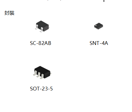
Automotive, 105��C Operation, 10 V Voltage Detector with Delay Function (External Delay Time Setting) S-19100xxxH Series Describe: The S-19100xxxH Series, developed by using CMOS technology, is a voltage detector IC for automotive 105��C operation. The detection voltage is fixed internally with an accuracy of ��2.5% (-Vdet = 2.4 V). It operates with current consumption of 270 nA typ. The release signal can be delayed by setting a capacitor externally, and the delay time accuracy at Ta = +25��C is ��15%. The operation temperature range is Ta = -40��C to +105��C. Two output forms Nch open-drain and CMOS output are available. Compared with conventional CMOS voltage detectors, the S-19100xxxH Series has super-low current consumption and small packages. Features: • Detection voltage: 1.2 V to 4.6 V (0.1 V step) • Detection voltage accuracy: ��2.5% (2.4 V �� −VDET �� 4.6 V, Ta = −40��C to +105��C) ��(2.0% + 12 mV) (1.2 V �� −VDET < 2.4 V, Ta = −40��C to +105��C) • Current consumption: 270 nA typ. (1.2 V �� −VDET < 2.3 V) • Operation voltage range: 0.6 V to 10.0 V (CMOS output product) • Hysteresis width*1: 5% ��2% (Ta = −40��C to +105��C) • Delay time accuracy: ��15% (CD = 4.7 nF, Ta = +25��C) • Output form: Nch open-drain output (active "L") CMOS output (active "L") • Operation temperature range: Ta = −40��C to +105��C • Lead-free (Sn 100%), halogen-free • AEC-Q100 qualified*2 *1. The product without hysteresis width is also available. *2. Contact our sales representatives for details. Applications: • For automotive use (meter, car body, headlight, ITS, accessory, car navigation system, car audio system, etc.) : SOT-23-5 package product, SC-82AB package product • For automotive use (accessory, car navigation system, car audio system, etc.) : SNT-4A package product |

|
S-191L/S-191NxxxxA
Automotive, 125��C Operation, 36 V, Supply Voltage Divided Output, Window Voltage Detector with SENSE Pin Reverse Connection Protection S-191L/191NxxxxA Series Describe: This IC, developed using CMOS technology, is a high-accuracy window voltage detector with the supply voltage divided output that detects undervoltage and overvoltage. The detection voltage and release voltage are fixed internally with an accuracy of ��1.5%. Apart from the power supply pin, the detection voltage input pin (SENSE pin) is also prepared, so the output is stable even if the SENSE pin voltage (VSENSE) falls to 0 V. The SENSE pin also has a built-in reverse connection protection circuit that reduces current in the SENSE pin during a reverse connection. The release signal can be delayed by setting a capacitor externally, and the release delay time accuracy is ��15% (CD = 3.3 nF). The output form is Nch open-drain output. The supply voltage divided output is prepared in this IC. The supply voltage divided output is a function that divides the VSENSE into VSENSE/6, VSENSE/8, VSENSE/12 or VSENSE/14 and outputs the voltage. For example, this function makes it possible that the IC connects to a low voltage microcontroller A/D converter directly and the microcontroller monitors a battery voltage. Features: Detector block • Detection voltage: Undervoltage detection voltage 4.0 V to 10.0 V (0.05 V step) Overvoltage detection voltage 16.0 V to 18.0 V (0.1 V step) • Detection voltage accuracy: Undervoltage detection voltage ��1.5% Overvoltage detection voltage ��1.5% • Hysteresis width selectable from "Available" / "Unavailable": "Available": 5.0%, 10.0% "Unavailable": 0% • Release delay time accuracy: ��15% (CD = 3.3 nF) • Output form: Nch open-drain output Supply voltage divider block • Output voltage: VPMOUT = VSENSE/6 (S-191L Series L / M / N type) VPMOUT = VSENSE/8 (S-191L Series P / Q / R type) VPMOUT = VSENSE/12 (S-191N Series L / M / N type) VPMOUT = VSENSE/14 (S-191N Series P / Q / R type) • Output capacitor (CPM): A ceramic capacitor can be used (0.1 ��F to 0.22 ��F). • Built-in enable circuit: Ensures long battery life. Overall • Current consumption: During supply voltage divided output operates 1.3 ��A typ. During supply voltage divided output stops 0.9 ��A typ. • Built-in reverse connection protection circuit: Reduces current in the SENSE pin during a reverse connection. • Operation voltage range: 3.0 V to 36.0 V • Operation temperature range: Ta = −40��C to +125��C • Lead-free (Sn 100%), halogen-free • Withstand 45 V load dump • AEC-Q100 qualified*1 *1. Contact our sales representatives for details. Applications: • Overvoltage detection of power supply for automotive electric component • Automotive battery voltage detection • For automotive use (engine, transmission, suspension, ABS, related-devices for EV / HEV / PHEV, etc.) |

|
S-191ExxxxA
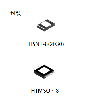
Automotive, 125��C Operation, 36 V, Window Voltage Detector with SENSE Pin Reverse Connection Protection S-191ExxxxA Series Describe: This IC, developed using CMOS technology, is a high-accuracy window voltage detector that detects undervoltage and overvoltage. The detection voltage and release voltage are fixed internally with an accuracy of ��1.5%. Apart from the power supply pin, the detection voltage input pin (SENSE pin) is also prepared, so the output is stable even if the SENSE pin voltage (VSENSE) falls to 0 V. The SENSE pin also has a built-in reverse connection protection circuit that reduces current in the SENSE pin during a reverse connection. The release signal can be delayed by setting a capacitor externally, and the release delay time accuracy is ��15% (CD = 3.3 nF). The output form is Nch open-drain output. Features: • Detection voltage: Undervoltage detection voltage 4.0 V to 10.0 V (0.05 V step) Overvoltage detection voltage 16.0 V to 18.0 V (0.1 V step) • Detection voltage accuracy: Undervoltage detection voltage ��1.5% Overvoltage detection voltage ��1.5% • Hysteresis width selectable from "Available" / "Unavailable": "Available": 5.0%, 10.0% "Unavailable": 0% • Release delay time accuracy: ��15% (CD = 3.3 nF) • Current consumption: 0.9 ��A typ. • Output form: Nch open-drain output • Built-in reverse connection protection circuit: Reduces current in the SENSE pin during a reverse connection. • Operation voltage range: 3.0 V to 36.0 V • Operation temperature range: Ta = −40��C to +125��C • Lead-free (Sn 100%), halogen-free • Withstand 45 V load dump • AEC-Q100 qualified*1 *1. Contact our sales representatives for details. Applications: • Overvoltage detection of power supply for automotive electric component • Automotive battery voltage detection • For automotive use (engine, transmission, suspension, ABS, related-devices for EV / HEV / PHEV, etc.) |
|
S-19117/19119xxxA Series
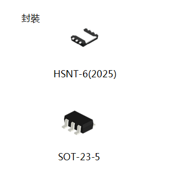
Automotive, 125��C Operation, 36 V, Supply Voltage Divided Output, Voltage Detector with SENSE Pin Reverse Connection Protection S-19117/19119xxxA Series Describes: This IC, developed using CMOS technology, is a high-accuracy voltage detector with the supply voltage divided output. The detection voltage and release voltage are fixed internally with an accuracy of ��1.5%. Apart from the power supply pin, the detection voltage input pin (SENSE pin) is also prepared, so the output is stable even if the SENSE pin voltage (VSENSE) falls to 0 V. The SENSE pin also has a built-in reverse connection protection circuit that reduces current in the SENSE pin during a reverse connection. The release signal can be delayed by setting a capacitor externally, and the release delay time accuracy is ��15% (CD =3.3 nF). The output form is Nch open-drain output. The supply voltage divided output is prepared in this IC. The supply voltage divided output is a function that divides the VSENSE into VSENSE/6, VSENSE/8, VSENSE/12 or VSENSE/14 and outputs the voltage. For example, this function makes it possible that the IC connects to a low voltage microcontroller A/D converter directly and the microcontroller monitors a battery voltage. Features: Detector block • Detection voltage: 4.0 V to 10.0 V (0.05 V step) • Detection voltage accuracy: ��1.5% • Hysteresis width selectable from "Available" / "Unavailable": "Available": 5.0%, 10.0% "Unavailable": 0% • Release delay time accuracy: ��15% (CD = 3.3 nF) • Output form: Nch open-drain output Supply voltage divider block • Output voltage: VPMOUT = VSENSE/6 (S-19117 Series L / M / N type) VPMOUT = VSENSE/8 (S-19117 Series P / Q / R type) VPMOUT = VSENSE/12 (S-19119 Series L / M / N type) VPMOUT = VSENSE/14 (S-19119 Series P / Q / R type) • Output capacitor (CPM): A ceramic capacitor can be used (0.1 ��F to 0.22 ��F). • Built-in enable circuit: Ensures long battery life. Overall • Current consumption: During supply voltage divided output operates 1.15 ��A typ. During supply voltage divided output stops 0.75 ��A typ. • Built-in reverse connection protection circuit: Reduces current in the SENSE pin during a reverse connection. • Operation voltage range: 3.0 V to 36.0 V • Operation temperature range: Ta = −40��C to +125��C • Lead-free (Sn 100%), halogen-free • Withstand 45 V load dump • AEC-Q100 qualified*1 *1. Contact our sales representatives for details. Applications: • Automotive battery voltage detection • For automotive use (engine, transmission, suspension, ABS, related-devices for EV / HEV / PHEV, etc.) |
|
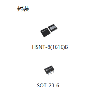
S-19114xxxA Series
Automotive, 125��C Operation, 36 V, Voltage Detector with Fast Detection Response, SENSE Pin Reverse Connection Protection, Delay Function (External Delay Time Setting) S-19114xxxA Series Describe: This IC, developed using CMOS technology, is a high-accuracy voltage detector. The detection voltage and release voltage are fixed internally with an accuracy of ��1.5%. Since the detection response time is as fast as 10 ��s max., voltage abnormalities can be detected and notified quickly. Apart from the power supply pin, the detection voltage input pin (SENSE pin) is also prepared, so the output is stable even if the SENSE pin voltage (VSENSE) falls to 0 V. The SENSE pin also has a built-in reverse connection protection circuit that reduces current in the SENSE pin during a reverse connection. The release signal can be delayed by setting a capacitor externally, and the release delay time accuracy is ��20% (CD = 3.3 nF). The output form is Nch open-drain output. Features: • Detection voltage: 4.0 V to 12.0 V (0.05 V step) • Detection voltage accuracy: ��1.5% • Hysteresis width selectable from "Available" / "Unavailable": "Available": 2.0%, 5.0%, 10.0% "Unavailable": 0% • Detection response time: 10 ��s max. (S-19114 Series L / M / N / R type) 25 ��s max. (S-19114 Series P / Q / S / T type) • Release delay time: 10 ms typ. (CD = 3.3 nF) • Release delay time accuracy: ��20% (CD = 3.3 nF) • Current consumption: 2.0 ��A typ. • Operation voltage range: 3.0 V to 36.0 V • Output form: Nch open-drain output • Built-in reverse connection protection circuit: Reduces current in the SENSE pin during a reverse connection. • Operation temperature range: Ta = −40��C to +125��C • Lead-free (Sn 100%), halogen-free • AEC-Q100 in process*1 *1. Contact our sales representatives for details. Applications: • Automotive battery voltage detection • For automotive use (engine, transmission, suspension, ABS, related-devices for EV / HEV / PHEV, etc.) |
|
S-191AxxxxA
Automotive, 125��C Operation, 6 V, Window Voltage Detector with Fast Detection Response and Manual Reset Function S-191AxxxxA Series Describes: This IC, developed using CMOS technology, is a high-accuracy window voltage detector that detects undervoltage and overvoltage. The detection voltage and release voltage are fixed internally with an accuracy of ��1.5%. Apart from the power supply pin, the detection voltage input pin (SENSE pin) is also prepared, so the output is stable even if the SENSE pin voltage (VSENSE) falls to 0 V. The release signal can be delayed by setting a capacitor externally, and the release delay time accuracy is ��15% (CD = 3.3 nF). This IC also has a manual reset function. The manual reset function changes the comparator input voltage of the internal circuit, and the detector is forcibly put into the detection status. This enables a diagnosis of anomalies in the detector, such as erroneous release. Features: • Detection voltage: Undervoltage detection voltage 0.6 V to 4.9 V (0.05 V step) Overvoltage detection voltage 0.7 V to 5.5 V (0.05 V step) • Detection voltage accuracy: Undervoltage detection voltage ��1.5% Overvoltage detection voltage ��1.5% • Hysteresis width selectable from "Available" / "Unavailable": "Available": 3.0%, 5.0%, 10.0% "Unavailable": 0% • Detection response time: 10.0 ��s typ. • Manual reset function: MR pin input logic: Active "L" • Release delay time accuracy: ��15% (CD = 3.3 nF) • Output form: Nch open-drain output • Current consumption: 1.5 ��A typ. • Operation voltage range: 2.5 V to 6.0 V • Operation temperature range: Ta = −40��C to +125��C • Lead-free (Sn 100%), halogen-free • AEC-Q100 in process*1 *1. Contact our sales representatives for details. Applications: • Overvoltage detection of power supply for automotive electric component • Voltage monitoring of automotive ECUs, ADAS and other systems that require failure detection • For automotive use (engine, transmission, suspension, ABS, related-devices for EV / HEV / PHEV, etc.) |

|
S-19122xxxA
Automotive, 125��C Operation, 6 V, Voltage Detector with Fast Detection Response and Manual Reset Function S-19122xxxA Series Describes�� This IC, developed using CMOS technology, is a high-accuracy voltage detector. The detection voltage and release voltage are fixed internally with an accuracy of ��1.5%. Apart from the power supply pin, the detection voltage input pin (SENSE pin) is also prepared, so the output is stable even if the SENSE pin voltage (VSENSE) falls to 0 V. The release signal can be delayed by setting a capacitor externally, and the release delay time accuracy is ��15% (CD = 3.3 nF). This IC also has a manual reset function. The manual reset function changes the comparator input voltage of the internal circuit, and the detector is forcibly put into the detection status. This enables a diagnosis of anomalies in the detector, such as erroneous release. Features: • Detection voltage: 0.6 V to 4.9 V (0.05 V step) • Detection voltage accuracy: ��1.5% • Hysteresis width selectable from "Available" / "Unavailable": "Available": 3.0%, 5.0%, 10.0% "Unavailable": 0% • Detection response time: 10.0 ��s typ. • Manual reset function: MR pin input logic: Active "L" • Release delay time accuracy: ��15% (CD = 3.3 nF) • Current consumption: 1.2 ��A typ. • Output form: Nch open-drain output • Operation voltage range: 2.5 V to 6.0 V • Operation temperature range: Ta = −40��C to +125��C • Lead-free (Sn 100%), halogen-free • AEC-Q100 in process*1 *1. Contact our sales representatives for details. Applications: • Voltage detection of power supply for automotive electric component • Voltage monitoring of automotive ECUs, ADAS and other systems that require failure detection • For automotive use (engine, transmission, suspension, ABS, related-devices for EV / HEV / PHEV, etc.) |

|
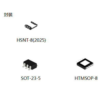
S-191BxxxxA
Automotive, 125��C Operation, 6 V, Window Voltage Detector with Fast Detection Response S-191BxxxxA Series Describes: This IC, developed using CMOS technology, is a high-accuracy window voltage detector that detects undervoltage and overvoltage. The detection voltage and release voltage are fixed internally with an accuracy of ��1.5%. Apart from the power supply pin, the detection voltage input pin (SENSE pin) is also prepared, so the output is stable even if the SENSE pin voltage (VSENSE) falls to 0 V. The release signal can be delayed by setting a capacitor externally, and the release delay time accuracy is ��15% (CD = 3.3 nF). Features: • Detection voltage: Undervoltage detection voltage 0.6 V to 4.9 V (0.05 V step) Overvoltage detection voltage 0.7 V to 5.5 V (0.05 V step) • Detection voltage accuracy: Undervoltage detection voltage ��1.5% Overvoltage detection voltage ��1.5% • Hysteresis width selectable from "Available" / "Unavailable": "Available": 3.0%, 5.0%, 10.0% "Unavailable": 0% • Detection response time: 10.0 ��s typ. • Release delay time accuracy: ��15% (CD = 3.3 nF) • Output form: Nch open-drain output • Current consumption: 1.5 ��A typ. • Operation voltage range: 2.5 V to 6.0 V • Operation temperature range: Ta = −40��C to +125��C • Lead-free (Sn 100%), halogen-free • AEC-Q100 in process*1 *1. Contact our sales representatives for details. Applications: • Overvoltage detection of power supply for automotive electric component • Voltage monitoring of automotive ECUs, ADAS, etc. • For automotive use (engine, transmission, suspension, ABS, related-devices for EV / HEV / PHEV, etc.) |
|
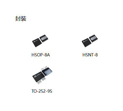
S-19720
Automotive, 125��C Operation, 36 V Input, 50 mA Voltage Tracker with Reverse Current Protection Function S-19720 Series. Describe: This IC, developed by using high-withstand voltage CMOS process technology, is a voltage tracker with a reverse current protection function, which has high-withstand voltage and low current consumption. Since the maximum operating voltage is as high as 36 V and the current consumption is as low as 30 ��A typ., it contributes to the reduction of standby current. This IC operates stably due to the internal phase compensation circuit so that users are able to use low ESR ceramic capacitor as the output capacitor. This IC includes an overcurrent protection circuit that prevents the load current from exceeding the current capacity of the output transistor and a thermal shutdown circuit that prevents damage because of overheating. Due to the built-in reverse current protection function, the reverse current flowing from the VOUT pin to the VIN pin can be controlled as the small value −5 ��A min. Therefore, IC protection diode is not needed. Features: • Input voltage: 4.0 V to 36.0 V • Offset voltage: ��5 mV(0.1 mA �� IOUT �� 50 mA) • Dropout voltage: 160 mV typ. (VADJ / EN = 4.0 V, IOUT = 10 mA) • Current consumption: During operation: 30 ��A typ. During power-off: 4.0 ��A typ. • Output current: Possible to output 50 mA (VIN = VADJ / EN + 2.0 V)*1 • Input capacitor: A ceramic capacitor can be used. (1.0 ��F or more) • Output capacitor: A ceramic capacitor can be used. (1.0 ��F to 1000 ��F) • Built-in overcurrent protection circuit: Limits overcurrent of output transistor. • Built-in thermal shutdown circuit: Detection temperature 175��C typ. • Reverse current protection function: IREV = −5 ��A min. (VIN = 0 V, VADJ / EN = 5.0 V, VOUT = 16.0 V) • Operation temperature range: Ta = −40��C to +125��C • Lead-free (Sn 100%), halogen-free • Withstand 45 V load dump • AEC-Q100 qualified*2 Applications: • Power supply for automotive off-board sensors • For automotive use (engine, transmission, suspension, ABS, related-devices for EV / HEV / PHEV, etc.) |
|
S-19721
Automotive, 125��C Operation, 36 V Input, 250 mA Voltage Tracker with Reverse Current Protection S-19721 Series Describe: This IC, developed by using high-withstand voltage CMOS process technology, is a voltage tracker with a reverse current protection function, which has high-withstand voltage and low current consumption. Since the maximum operating voltage is as high as 36 V and the current consumption is as low as 40 ��A typ., it contributes to the reduction of standby current. This IC operates stably due to the internal phase compensation circuit so that users are able to use low ESR ceramic capacitor as the output capacitor. Features: • Input voltage: 4.0 V to 36.0 V • Output voltage: Adjustable down to 2.0 V min. • Offset voltage: ��4.5 mV (0.1 mA �� IOUT �� 250 mA) • Dropout voltage: 330 mV typ. (VADJ = 4.0 V, IOUT = 125 mA) • Current consumption: During operation: 40 ��A typ. During power-off: 3.7 ��A typ. • Output current: Possible to output 250 mA (VIN = VADJ + 2.0 V)*1 • Input capacitor: A ceramic capacitor can be used. (4.7 ��F or more) • Output capacitor: A ceramic capacitor can be used. (4.7 ��F to 1000 ��F) • Built-in overcurrent protection circuit: Limits overcurrent of output transistor. • Built-in thermal shutdown circuit: Detection temperature 175��C typ. • Built-in overvoltage detection circuit: Detects an output short-circuit of the higher voltage. • Reverse current protection function: IREV = −5 ��A min. (VIN = 0 V, VADJ = 5.0 V, VOUT = 16.0 V) • INT pin output function: Able to monitor the operating status of the IC • Operation temperature range: : Ta = −40��C to +125��C • Lead-free (Sn 100%), halogen-free • Withstand 45 V load dump • AEC-Q100 in process*2 *1. Please make sure that the loss of the IC will not exceed the power dissipation when the output current is large. *2. Contact our sales representatives for details. Applications: • Power supply for automotive off-board sensors • For automotive use (engine, transmission, suspension, ABS, related-devices for EV / HEV / PHEV, etc.) |
|
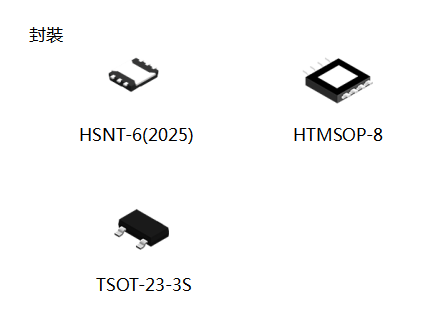
S-57TZ S
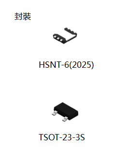
Automotive, 150��C Operation, High-Withstand Voltage, High-Speed, ZCL™ Hall Effect IC S-57TZ S Series Describe: This IC, developed by CMOS technology, is a high-accuracy Hall effect IC that operates with high temperature and high-withstand voltage. The IC switches output voltage level when the IC detects magnetic flux density (magnetic field) polarity changes. The ZCL (Zero Crossing Latch) detection method realizes polarity changes detection with the higher accuracy than the conventional bipolar latch method. Using this IC with a magnet makes it possible to detect the rotation status in various devices. Features: Uses a thin (t0.80 mm max.) TSOT-23-3S or ultra-thin (t0.50 mm max.) HSNT-6(2025) package, allowing for device miniaturization Contributes to reduction of mechanism operation dispersion through high accuracy detection of magnetic flux density (magnetic field) polarity changes Suitable for devices which require high quality due to the production system of this IC which certifies automotive application quality Contributes to device safe design with a built-in reverse voltage protection circuit and output current limit circuit Applications: Brushless DC (BLDC) motor for automotive applications Automobile equipment Housing equipment Industrial equipment |
|
S-57RB S
Automotive, 150��C Operation, High-Withstand Voltage, High-Speed, Bipolar Hall Effect Latch IC S-57RB S Series Describe�� This IC, developed by CMOS technology, is a high-accuracy Hall effect latch IC that operates with high temperature and high-withstand voltage. The output voltage level changes when this IC detects the intensity level of magnetic flux density and a polarity change. Using this IC with a magnet makes it possible to detect the rotation status in various devices. Features : Uses a thin (t0.80 mm max.) TSOT-23-3S or ultra-thin (t0.50 mm max.) HSNT-6(2025) package, allowing for device miniaturization Contributes to reduction of mechanism operation dispersion with high-accuracy magnetic characteristics (Typ. value �� 1.0 mT) (Refer to ��Magnetic Characteristics�� in the datasheet for details.) Our production system certifies automotive application quality, which allows for use in devices which require high quality Contributes to device safe design with a built-in reverse voltage protection circuit and output current limit circuit. Applications: DC brushless motor for automotive applications Automobile equipment Housing equipment Industrial equipment |

|
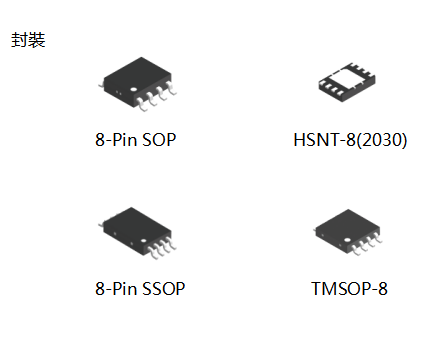
S-25A010A/S-25A020A/S-25A040A
125��C Operation SPI Serial EEPROM for Automotive S-25A010A/020A/040A (1K/2K/4K-bit) Describe: This IC is a SPI serial E2 PROM which operates under the high temperature, at high speed, with the wide range operation for automotive components. This IC has the capacity of 1 K-bit, 2 K-bit, 4 K-bit and the organization of 128 words �� 8-bit, 256 words �� 8-bit, 512 words �� 8-bit. Page write and Sequential read are available. Features:
Read: 2.5 V to 5.5 V Write: 2.5 V to 5.5 V
6.5 MHz max.
Software, Hardware Protect area: 25%, 50%, 100%
106cycles/word*1 (Ta =��25��) 5 �� 105cycle / word*1 (Ta =��125��)
100 years (Ta =��25��) 50 years (Ta =��125��)
S-25A010A: 1 Kbit S-25A020A: 2 Kbit S-25A040A: 4 Kbit
*1. For each address (Word: 8 bits) *2. Contact our sales representatives for details. |

|
S-25A080/S-25A160/S-25A320
125��C Operation SPI Serial EEPROM for Automotive S-25A080A / 160A / 320A, S-25A080B / 160B / 320B (8K / 16K / 32K-bit) Describe: This IC is a SPI serial E2 PROM which operates under the high temperature, at high speed, with the wide range operation for automotive components. This IC has the capacity of 8 K-bit, 16 K-bit, 32 K-bit and the organization of 1024 words �� 8-bit, 2048 words �� 8-bit, 4096 words �� 8-bit. Page write and Sequential read are available. Features:
Read: 2.5 V ~ 5.5 V Write: 2.5 V ~ 5.5 V
S-25A080A/160A/320A: 4.0 ms max. S-25A080B/160B/320B: 5.0 ms max.
S-25A080A/160A/320A : 106�� / ��*2 (Ta = +25��)��5��105 �� / ��*2 (Ta = +125��) S-25A080B/160B/320B : 106�� / ��*2 (Ta = +25��)��3��105 �� / ��*2 (Ta = +125��)
100 years (Ta =+25��) 50 years (Ta =+125��)
S-25A080A, S-25A080B: 8 K-bit S-25A160A, S-25A160B: 16 K-bit S-25A320A, S-25A320B: 32 K-bit
*1. Refer to "��Endurance" for details. *2. For each address (Word: 8-bit) *3. Refer to "��Product Name Structure" for details. *4. Contact our sales office for details. |

|
S-25A640A/S-25A640B
125��C Operation SPI Serial EEPROM for Automotive S-25A640A, S-25A640B (64K-bit) Describe: This IC is a SPI serial E2 PROM which operates under the high temperature, at high speed, with the wide range operation for automotive components. This IC has the capacity of 64 K-bit and the organization of 8192 words 8-bit. Page write and Sequential read are available. Features:
Read: 2.5 V ~ 5.5 V Write: 2.5 V ~ 5.5 V
S-25A640A: 5.0 MHz max. S-25A640B: 6.5 MHz max.
S-25A640A: 4.0 ms max. S-25A640B: 5.0 ms max.
Protect area: 25%, 50%, 100%
S-25A640A : 106 �� / ��*2 (Ta = +25��)��5 �� 105 �� / ��*2 (Ta = +125��) S-25A640B : 106 �� / ��*2 (Ta = +25��)��3 �� 105 �� / ��*2 (Ta = +125��)
100 years (Ta = +25��) 50 years (Ta = +125��)
*1. Refer to "��Endurance" for details. *2. For each address (Word: 8-bit) *3. Refer to "��Product Name Structure" for details. *4. Contact our sales office for details. |
|
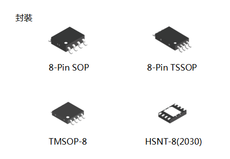
S-93C46C/S-93C56C/S-93C66C/S-93C76C/S-93C86C H
Automotive 105��C Operation 3-wire Serial EEPROM S-93C46C / 56C / 66C / 76C / 86C H Series Describe: This IC is a high speed, low current consumption, 3-wire serial EEPROM with a wide operating voltage range. This IC has the capacity of 1 K-bit, 2 K-bit, 4 K-bit, 8 K-bit and 16 K-bit, and the organization is 64 words �� 16-bit, 128 words �� 16-bit, 256 words �� 16-bit, 512 words �� 16-bit and 1024 words �� 16-bit, respectively. Sequential read is available, at which time addresses are automatically incremented in 16-bit blocks. The communication method is by the Microwire bus. Features: • Memory capacity S-93C46C: 1 K-bit (64-word �� 16-bit) S-93C56C: 2 K-bit (128-word �� 16-bit) S-93C66C: 4 K-bit (256-word �� 16-bit) S-93C76C: 8 K-bit (512-word �� 16-bit) S-93C86C: 16 K-bit (1024-word �� 16-bit) • Operation voltage range Read: 1.6 V to 5.5 V Write: 1.8 V to 5.5 V • Operation frequency: 2.0 MHz max. • Write time: 4.0 ms max. • Sequential read • Write protect function during the low power supply voltage • Function to protect against write due to erroneous instruction recognition • Endurance: 106 cycle / word*1 (Ta = +85��C) 8 �� 105 cycle / word*1 (Ta = +105��C) • Data retention: 100 years (Ta = +25��C) 50 years (Ta = +105��C) • Initial delivery state: FFFFh • Operation temperature range: Ta = −40��C to +105��C • Lead-free (Sn 100%), halogen-free • AEC-Q100 qualified*2 *1. For each address (Word: 16-bit) *2. Contact our sales representatives for details. |
|
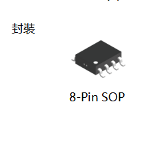
S-93A46B/S-93A56B/S-93A66B/S-93A76B/S-93A86B
Automotive 125��C Operation 3-wire Serial EEPROM S-93A46B/56B/66B/76B/86B Describe: This IC is a high temperature operation 3-wire serial EEPROM for automotive components. This IC has the capacity of 1 K-bit, 2 K-bit, 4 K-bit, 8 K-bit and 16 K-bit, and the organization is 64 words �� 16-bit, 128 words �� 16-bit, 256 words �� 16-bit, 512 words �� 16-bit and 1024 words �� 16-bit, respectively. Sequential read is available, at which time addresses are automatically incremented in 16-bit blocks. The communication method is by the Microwire bus. Features: • Memory capacity S-93A46B: 1 K-bit (64-word �� 16-bit) S-93A56B: 2 K-bit (128-word �� 16-bit) S-93A66B: 4 K-bit (256-word �� 16-bit) S-93A76B: 8 K-bit (512-word �� 16-bit) S-93A86B: 16 K-bit (1024-word �� 16-bit) • Operation voltage range Read: 2.5 V to 5.5 V Write: 2.5 V to 5.5 V • Operation frequency: 2.0 MHz max. • Write time: 4.0 ms max. • Sequential read • CMOS schmitt input (CS, SK, DI) • Write protect function during the low power supply voltage • Function to protect against write due to erroneous instruction recognition • Endurance: 106 cycle / word*1 (Ta = +85��C) 8 �� 105 cycle / word*1 (Ta = +105��C) 5 �� 105 cycle / word*1 (Ta = +125��C) • Data retention: 100 years (Ta = +25��C) 50 years (Ta = +125��C) • Initial delivery state: FFFFh • Wafer level burn-in (standard specification) • Operation temperature range: Ta = −40��C to +125��C • Lead-free (Sn 100%), halogen-free • AEC-Q100 qualified*2 *1. For each address (Word: 16-bit) *2. Contact our sales representatives for details. |
|
S-93S46A/S-93S56A/S-93S66A
For Automotive 150��C Operation 3-Wire Serial EEPROM S-93S46A/56A/66A Describe: This IC is a high temperature operation 3-wire serial EEPROM for automotive components. This IC has the capacity of 1K-bit, 2K-bit, and 4K-bit and the organization is 64 words��16-bit, 128 words��16-bit and 256 words��16-bit respectively. Sequential read is available, at which time addresses are automatically incremented in 16-bit blocks. The communication method is by the Microwire bus. Features: • Operation voltage range Read: 4.0 V to 5.5 V (Ta = −40��C to +150��C) Write: 4.0 V to 5.5 V (Ta = −40��C to +150��C) • Operation frequency: 1 MHz (4.5 V to 5.5 V, Ta = −40��C to +150��C) • Write time: 10.0 ms max. • Sequential read • Write protect function during the low power supply voltage • Function to protect against write due to erroneous instruction recognition • CMOS schmitt input (CS, SK) • Endurance*1: 2 �� 105 cycle / word*2 (Ta = +150��C) • Data retention: 100 years (Ta = +25��C) 50 years (Ta = +125��C) 20 years (Ta = +150��C) • Memory capacity S-93S46A: 1 K-bit S-93S56A: 2 K-bit S-93S66A: 4 K-bit • Initial delivery state: FFFFh • Burn-in specification: Wafer level burn-in • Operation temperature range: Ta = −40��C to +150��C • Lead-free (Sn 100%), halogen-free • AEC-Q100 qualified*3 *1. Refer to "��Endurance" for details. *2. For each address (Word: 16-bit) *3. Contact our sales representatives for details. |

|
S-24C08C H
105��C Operation 2-wire Serial EEPROM for Automotive S-24C08C H Series (8K-bit) Describe: The S-24C08C H series is a high temperature operation 2-wire serial E2 PROMs for automotive components. The S-24C08C H series has the capacity of 8 K-bit, and the organization is 1024 words 8-bit. Page write and sequential read are available. Features:
Read 2.5 V to 5.5 V Write 2.5 V to 5.5 V
106 cycles / word*1 (Ta = +25��C) 3��105cycles / word*1 (Ta = +85��C) 2��105cycles / word*1 (Ta = +105��C)
30 years (Ta = +85��C) 25 years (Ta = +105��C)
*1. For each address (Word: 8-bit) *2. Contact our sales office for details |
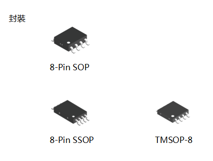
|
S-24C16C H
105��C Operation 2-wire Serial EEPROM for Automotive S-24C16C H Series (16K-bit) Describe: The S-24C16C H series is a high temperature operation 2-wire serial E2PROM for automotive components. The S-24C16C H series has the capacity of 16 K-bit, and the organization is 2048 words �� 8- bit. Page write and sequential read are available. Features:
Read 2.5 V to 5.5 V Write 2.5 V to 5.5 V
106 cycles / word*1 (Ta = +25��C) 3��105cycles / word*1 (Ta = +85��C) 2��105cycles / word*1 (Ta = +105��C)
30 years (Ta = +85��C) 25 years (Ta = +105��C)
*1. For each address (Word: 8-bit) *2. Contact our sales office for details |

|
S-24C32C/S-24C64C H
105��C Operation 2-wire Serial EEPROM for Automotive S-24C32C/64C H Series (32K/64K-bit) Describe: The S-24C32C/64C H series is a high temperature operation 2-wire serial EEPROM for automotive components. The S-24C32C/64C H series has the capacity of 32 K-bit and 64 K-bit, and the organization is 4096 words �� 8-bit, 8192 words �� 8-bit, respectively. Page write and sequential read are available. Features:
Read 2.5 V to 5.5 V Write 2.5 V to 5.5 V
106 cycles / word*1 (Ta = +25��C) 3��105cycles / word*1 (Ta = +85��C) 2��105cycles / word*1 (Ta = +105��C)
30 years (Ta = +85��C) 25 years (Ta = +105��C)
S-24C32C 32 K-bit S-24C64C 64 K-bit
*1. For each address (Word: 8-bit) *2. Contact our sales office for details |

|
S-24C128C H
105��C Operation 2-wire Serial EEPROM for Automotive S-24C128C H Series (128K-bit) Describe: The S-24C128C H series is a high temperature operation 2-wire serial EEPROM for automotive components. The S-24C128C H series has the capacity of 128 K-bit, and the organization is 16384 words �� 8-bit. Page write and sequential read are available. Features: • Operating voltage range: Read 2.5 V to 5.5 V Write 2.5 V to 5.5 V • Page write: 64 bytes / page • Sequential read • Operation frequency: 400 kHz (VCC = 2.5 V to 5.5 V) • Write time: 5.0 ms max. • Noise suppression: Schmitt trigger and noise filter on input pins (SCL, SDA) • Write protect function during the low power supply voltage • Endurance: 106 cycles/word*1 (Ta = +25��C) 3 �� 105 cycles/word*1 (Ta = +85��C) 2 �� 105 cycles/word*1 (Ta = +105��C) • Data retention: 100 years (Ta = +25��C) 30 years (Ta = +85��C) 25 years (Ta = +105��C) • Memory capacity: 128 K-bit • Write protect: 100% • Initial delivery state: FFh • Operation temperature range: Ta = −40��C to +105��C • Lead-free (Sn 100%), halogen-free • AEC-Q100 qualified*2 *1. For each address (Word: 8-bit) *2. Contact our sales office for details. |

|
S-25C010A/S-25C020A/S-25C040A H
105��C Operation SPI Serial EEPROM for Automotive S-25C010A/020A/040A H Series (1K/2K/4K-bit) Describe: The S-25C010A/020A/040A H series devices are hightemperature operation SPI serial E2PROMs for automotive components. The S-25C010A/020A/040A H series has the capacity of 1 K-bit, 2 K-bit, and 4 K-bit, and the organization is 128 words �� 8-bit, 256 words �� 8- bit, and 512 words �� 8- bit, respectively. Page write and sequential read are available. Features:
Read 2.5 V to 5.5 V Write 2.5 V to 5.5 V
106cycles/word*1 (Ta = 85��C) 8 �� 105 cycles/word*1 (Ta = +105��C)
100 years (Ta = +25��C) 50 years (Ta = +105��C)
S-25C010A 1 K-bit S-25C020A 2 K-bit S-25C040A 4 K-bit
*1. For each address (Word: 8-bit) *2. Contact our sales office for details. |
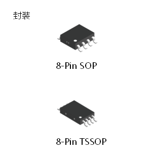
|
S-25C080A H
105��C Operation SPI Serial EEPROM for Automotive S-25C080A H Series (8K-bit) Describe: The S-25C080A H series devices are high-temperature operation SPI serial E2PROMs for automotive components. The S- 25C080A H series has the capacity of 8 K-bit and the organization is 1024 words �� 8-bit. Page write and sequential read are available. Features: • Operating voltage range: Read 2.5 V to 5.5 V Write 2.5 V to 5.5 V • Operation frequency: 6.5 MHz (4.5 V to 5.5 V) • Write time: 4.0 ms max. • SPI mode (0, 0) and (1, 1) • Page write 32 bytes / page • Sequential read • Monitors write to the memory by a status register • Write protect: Software, Hardware • Protect area: 25%, 50%, 100% • Function to prevent malfunction by monitoring clock pulse • Write protect function during the low power supply voltage • CMOS schmitt input ( CS , SCK, SI, WP , HOLD ) • Endurance: 106 cycles/word*1 (Ta = +85��C) 8 �� 105 cycles/word*1 (Ta = +105��C) • Data retention: 100 years (Ta = +25��C) 50 years (Ta = +105��C) • Memory capacitance: 8 K-bit • Initial delivery state: FFh, SRWD = 0, BP1 = 0, BP0 = 0 • Operation temperature range: Ta = −40��C to +105��C • Lead-free (Sn 100%), halogen-free • AEC-Q100 qualified*2 *1. For each address (Word: 8-bit) *2. Contact our sales office for detail |
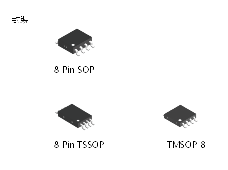
|
S-25C160A H
105��C Operation SPI Serial EEPROM for Automotive S-25C160A H Series (16K-bit) Describe: The S-25C160A H series devices are high-temperature operation SPI serial EEPROMs for automotive components. The S- 25C160A H series has the capacity of 16 K-bit and the organization of 2048 words �� 8-bit. Page write and sequential read are available. Features:
Read 2.5 V to 5.5 V Write 2.5 V to 5.5 V
106cycles/word*1 (Ta = +25��C) 3 �� 105cycles/word*1 (Ta = +85��C) 2 �� 105cycles/word*1 (Ta = +105��C)
100 years (Ta = +25��C) 30 years (Ta = +85��C) 25 years (Ta = +105��C)
*1. For each address (Word: 8-bit) *2. Contact our sales office for details. |

|
S-25C128A H
105��C Operation SPI Serial EEPROM for Automotive S-25C128A H Series (128K-bit) Describe: The S-25C128A H series devices are high-temperature operation SPI serial EEPROMs for automotive components. The S- 25C128A H series has the capacity of 128 K-bit and the organization of 16384 words �� 8-bit. Page write and sequential read are available. Features: • Operating voltage range: Read 2.5 V to 5.5 V Write 2.5 V to 5.5 V • Operation frequency: 5.0 MHz (2.5 V to 5.5 V) • Write time: 5.0 ms max. • SPI mode (0, 0) and (1, 1) • Page write: 64 bytes / page • Sequential read • Monitors write to the memory by a status register • Write protect: Software, Hardware Protect area: 25%, 50%, 100% • Function to prevent malfunction by monitoring clock pulse • Write protect function during the low power supply voltage • CMOS schmitt input ( CS , SCK, SI, WP , HOLD ) • Endurance: 106 cycles/word*1 (Ta = +25��C) 3 �� 105 cycles/word*1 (Ta = +85��C) 2 �� 105 cycles/word*1 (Ta = +105��C) • Data retention: 100 years (Ta = +25��C) 30 years (Ta = +85��C) 25 years (Ta = +105��C) • Memory capacitance: 128 K-bit • Initial delivery state: FFh, SRWD = 0, BP1 = 0, BP0 = 0 • Operation temperature range: Ta = −40��C to +105��C • Lead-free (Sn 100%), halogen-free • AEC-Q100 qualified*2 *1. For each address (Word: 8-bit) *2. Contact our sales office for details. |
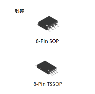
|
S-25A128B
125��C Operation SPI Serial EEPROM for Automotive S-25A128B Describe: This IC is a SPI serial EEPROM which operates under the high temperature, at high speed, with the wide range operation for automotive components. This IC has the capacity of 128 K-bit and the organization of 16384 words �� 8-bit. Page write and Sequential read are available. Features:
Read: 2.5 V ~ 5.5 V Write: 2.5 V ~ 5.5 V
Software, Hardware Protect area: 25%, 50%, 100%
106cycle / word*2 (Ta = +25��) 3 �� 105cycle / word *2 (Ta = +125��)
100 years (Ta = +25��) 50 years (Ta = +125��)
*1. Refer to "��Endurance" for details. *2. For each address (Word: 8-bit) *3. Refer to "��Product Name Structure" for details. *4. Contact our sales office for details. |
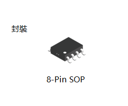
|
S-25A256B
125��C Operation SPI Serial EEPROM for Automotive S-25A256B Describe: This IC is a SPI serial EEPROM which operates under the high temperature, at high speed, with the wide range operation for automotive components. This IC has the capacity of 256 K-bit and the organization of 32768 words �� 8-bit. Page write and Sequential read are available. Features:
Read: 2.5 V ~ 5.5 V Write: 2.5 V ~ 5.5 V
Software, Hardware Protect area: 25%, 50%, 100%
106cycle / word *2 (Ta = +25��C) 3 �� 105cycle / word *2 (Ta = +125��C)
100 years (Ta = +25��C) 50 years (Ta = +125��C)
*1. Refer to "��Endurance" for details. *2. For each address (Word: 8-bit) *3. Refer to "��Product Name Structure" for details. *4. Contact our sales office for details. |
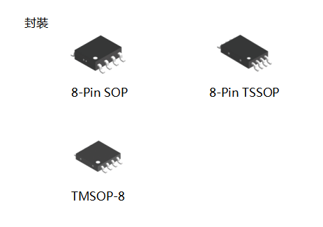
|
S-25C320A/640A H
The S-25C320A/640A H series devices are high-temperature operation SPI serial EEPROMs for automotive components. The S-25C320A/640A H series has the capacity of 32 K-bit and 64 Kbit, and the organization is 4096 words �� 8-bit, 8192 words �� 8- bit, respectively. Features: �� Operating voltage range: Read 2.5 V to 5.5 V Write 2.5 V to 5.5 V �� Operation frequency: 5.0 MHz (2.5 V to 5.5 V) �� Write time: 5.0 ms max. �� SPI mode (0, 0) and (1, 1) �� Page write 32 bytes / page �� Sequential read �� Monitors write to the memory by a status register �� Write protect: Software, Hardware Protect area: 25%, 50%, 100% �� Function to prevent malfunction by monitoring clock pulse �� Write protect function during the low power supply voltage �� CMOS schmitt input ( CS , SCK, SI, WP , HOLD ) �� Endurance: 106cycles/word*1 (Ta = -25��C) 3��105cycles/word*1 (Ta = +85��) 2��105cycles/word*1 (Ta = +105��C) �� Data retention: 100 years (Ta = -25��C) 30 years (Ta = +85��C) 25 years (Ta = +105��C) �� Memory capacitance: S-25C320A 32 K-bit S-25C640A 64 K-bit �� Initial delivery state: FFh, SRWD = 0, BP1 = 0, BP0 = 0 �� Operation temperature range: Ta = -40��C to +105��C �� Lead-free (Sn 100%), halogen-free �� AEC-Q100 qualified*2 *1. For each address (Word: 8-bit) *2. Contact our sales office for details. |
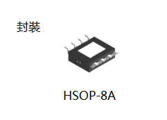
|
S-19700
Automotive, 125��C Operation, 36 V Input, 400 mA Voltage Regulator with Current Monitor And Adjustable Current Limit S-19700 Series Describe: The S-19700 Series, developed by using CMOS technology, is a positive voltage regulator with a current monitoring function for 125��C automotive operation. It provides an output current of 400 mA min., and a ceramic capacitor of 4.7 ��F or more can be used as the output capacitor. Due to the built-in reverse current protection function, the reverse current flowing from the VOUT pin to the VIN pin can be controlled as the small value 15 ��A typ. The current monitor monitors the current flowing to the voltage regulator and outputs the voltage according to the external resistance, and limits the current value from exceeding the set value. The S-19700 Series has two types of products of which one is the externally set product whose output voltage is determined by the external divided-resistor, and the other is the internally set product which includes an INT pin and whose output voltage is fixed. Features:
During operation: 80 ��A typ., 170 ��A max. (Tj = −40��C to +150��C) During power-off: 1.0 ��A typ., 5.0 ��A max. (Tj = −40��C to +90��C)
*1. Please make sure that the loss of the IC will not exceed the power dissipation when the output current is large. *2. Contact our sales representatives for details. Applications:
|
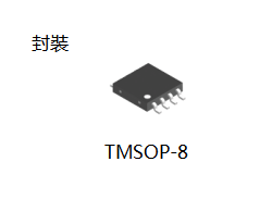
|
S-19680
Automotive, 105��C Operation, High Side Switch with Current Monitor S-19680 Series Describe: The S-19680 Series, developed by using CMOS technology, is a high side switch with the current monitor function. When the Pch output transistor is turned on, voltage is supplied to the load connected to the OUT pin. Monitoring the current which flows from the VIN pin to the OUT pin by using two external resistors, the S-19680 Series limits the current so that it does not exceed the set value. Depending on the monitored current value, the S-19680 Series detects the short-circuit status or the open status of the load connected to the OUT pin, and outputs an alarm signal. In addition, the S-19680 Series has the ON / OFF circuit to control the Pch output transistor��s status, ON and OFF, and the thermal shutdown circuit to limit overheating. The hysteresis type or latch type can be selected for the thermal shutdown circuit. Features: • Power supply voltage: VDD = 2.7 V to 10.0 V • Current consumption during operation: ISS1 = 12 ��A typ., ISS1 = 24 ��A max. (Tj = −40��C to +105��C) • ON resistance: RON = 1.1 �� typ., RON = 3.7 �� max. (Tj = −40��C to +105��C) • Limit current: 40 mA to 100 mA, selectable in 10 mA step • Load short-circuit detection current: ILIM �� 0.3 to ILIM �� 1.0 (ISHORT �� 30 mA), selectable in 0.1 step • Load open detection current: 2.5 mA to 30 mA, selectable in 2.5 mA step • Built-in thermal shutdown circuit: Detection temperature 165��C typ. Selectable in hysteresis type or latch type • Built-in ON / OFF circuit: Ensures long battery life. • Operation temperature range: Ta = −40��C to +105��C • Lead-free (Sn 100%), halogen-free • AEC-Q100 qualified*1 *1. Contact our sales representatives for details. Applications�� • Remote LNA phantom power such as GPS antenna • ADAS locator • e-call • Car navigation system • Car audio system |

|
S-19701
Automotive, 125��C Operation, 36 V Input, 600 mA Voltage Regulator with Current Monitor And Adjustable Current Limit S-19701 Series Describe: The S-19701 Series, developed by using CMOS technology, is a positive voltage regulator with a current monitoring function for 125��C automotive operation. It provides an output current of 600 mA min., and a ceramic capacitor of 4.7 ��F or more can be used as the output capacitor. Due to the built-in reverse current protection function, the reverse current flowing from the VOUT pin to the VIN pin can be controlled as the small value 15 ��A typ. The current monitor monitors the current flowing to the voltage regulator and outputs the voltage according to the external resistance, and limits the current value from exceeding the set value. The S-19701 Series has two types of products of which one is the externally set product whose output voltage is determined by the external divided-resistor, and the other is the internally set product which includes an INT pin and whose output voltage is fixed. By connecting the VADJ pin to GND, the externally set product can be utilized as a high side switch with a current monitor. Features:
During operation: 80 ��A typ., 170 ��A max. (Tj = −40��C to +150��C) During power-off: 1.0 ��A typ., 5.0 ��A max. (Tj = −40��C to +90��C)
*1. Please make sure that the loss of the IC will not exceed the power dissipation when the output current is large. *2. Contact our sales representatives for details. Applications:
|

|
S-19682B
Automotive, 125��C Operation, 36 V Input, 300 mA, High Side Switch with Current Monitor S-19682B Series Describe: This IC, developed by using CMOS technology, is a high side switch with the current monitor function. When the Pch output transistor is turned on, voltage is supplied to the load connected to the VOUT pin. The current monitor measures the current flowing to the high side switch, outputs the voltage according to the load current, and limits the current value from exceeding the set value. In addition, this IC has the ON / OFF circuit to control the Pch output transistor��s status, ON and OFF, and the thermal shutdown circuit to limit overheating. Features: • Input voltage: 4.5 V to 36.0 V • Current consumption: During operation: 55 ��A typ., 95 ��A max. (Tj = −40��C to +150��C) During power-off: 0.6 ��A typ., 2.0 ��A max. (Tj = −40��C to +125��C) • ON resistance: RON = 0.6 �� typ., 1.0 �� max. (Tj = −40��C to +125��C) • Limit current: 100 mA to 300 mA, selectable in 10 mA step • Limit current accuracy: ��10% (ILIM(S) = 200 mA to 300 mA) • Current monitor function: Possible to monitor load current by monitoring the CSO pin voltage. • Built-in thermal shutdown circuit: Latch type*1, detection temperature 170��C typ. • Build-in overvoltage detection circuit: Detects an output short-circuit of the higher voltage. • Built-in ON / OFF circuit: Ensures long battery life. • Under voltage lockout function (UVLO): 2.6 V typ. (Detection voltage) • Operation temperature range: Ta = −40��C to +125��C • Lead-free (Sn 100%), halogen-free • Withstand 45 V load dump • AEC-Q100 qualified*2 *1. Please contact our sales representatives for products with hysteresis type. *2. Contact our sales office for details. Applications: • Remote LNA phantom power such as GPS antenna • ADAS locator • e-call • Car navigation system • Car audio system |

|
S-19683B
Automotive, 125��C Operation, 36 V Input, 600 mA, High Side Switch with Current Monitor S-19683B Series Describe: This IC, developed by using CMOS technology, is a high side switch with the current monitor function. When the Pch output transistor is turned on, voltage is supplied to the load connected to the VOUT pin. The current monitor measures the current flowing to the high side switch, outputs the voltage according to the load current, and limits the current value from exceeding the set value. In addition, this IC has the ON / OFF circuit to control the Pch output transistor��s status, ON and OFF, and the thermal shutdown circuit to limit overheating. Features: • Input voltage: 4.5 V to 36.0 V • Current consumption: During operation: 55 ��A typ., 95 ��A max. (Tj = −40��C to +150��C) During power-off: 0.6 ��A typ., 2.0 ��A max. (Tj = −40��C to +125��C) • ON resistance: RON = 0.6 �� typ., 1.0 �� max. (Tj = −40��C to +125��C) • Limit current: 300 mA to 600 mA, selectable in 10 mA step • Limit current accuracy: ��10% • Current monitor function: Possible to monitor load current by monitoring the CSO pin voltage. • Built-in thermal shutdown circuit: Latch type*1, detection temperature 170��C typ. • Build-in overvoltage detection circuit: Detects an output short-circuit of the higher voltage. • Built-in ON / OFF circuit: Ensures long battery life. • Under voltage lockout function (UVLO): 2.6 V typ. (Detection voltage) • Operation temperature range: Ta = −40��C to +125��C • Lead-free (Sn 100%), halogen-free • Withstand 45 V load dump • AEC-Q100 qualified *2 *1. Please contact our sales representatives for products with hysteresis type. *2. Contact our sales office for details. Applications: • Automotive surround camera ECU • Connection diagnosis for camera module |
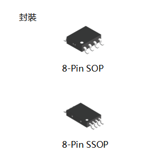
|
S-35390A H
For Automotive 105��C 2-wire Real-time Clock S-35390A H Series Describe: The S-35390A H Series is a CMOS 2-wire real-time clock IC which operates with the very low current consumption, 105��C operation in the wide range of operation voltage. The operation voltage is 1.3 V to 5.5 V so that the S-35390A H Series can be used for various power supplies from main supply to backup battery. Due to the 0.25 ��A current consumption and wide range of power supply voltage at time keeping, the S-35390A H Series makes the battery life longer. In the system which operates with a backup battery, the included free registers can be used as the function for user��s backup memory. Users always can take back the information in the registers which is stored before power-off the main power supply, after the voltage is restored. The S-35390A H Series has the function to correct advance / delay of the clock data speed, in the wide range, which is caused by the oscillation circuit��s frequency deviation. Correcting according to the temperature change by combining this function and a temperature sensor, it is possible to make a high precise clock function which is not affected by the ambient temperature. Features:
*1. Contact our sales office for details. |
|
S-19630A
Automotive, 125��C Operation, Low Input Offset Voltage CMOS Operational Amplifier S-19630A Describe: This IC incorporates a general purpose analog circuit in a small package. This is a zero-drift operational amplifier with Rail-to-Rail input and output, which uses chopper-stabilizing techniques to provide low input offset voltage. The S-19630AB is a dual operational amplifier (2 circuits), which is suitable for applications requiring less offset voltage.
Features: • Low input offset voltage: VIO = +50 ��V max. (Ta = −40��C to +125��C) • Low input offset voltage drift: ��VIO/��Ta = ��25 nV/��C typ. (VDD = 30.0 V, Ta = −40��C to +125��C) • Operation power supply voltage range: VDD = 4.0 V to 36.0 V • Low current consumption (Per circuit): IDD = 250 ��A typ. • Low input noise voltage: VNOISE_pp = 0.8 ��Vpp typ. (f = 0.1 Hz to 10 Hz) • Low input noise voltage density: VNOISE = 25 nV/��Hz typ. (f = 1 kHz) • Built-in output current limit circuit: Overcurrent limit when output pin is short-circuited • Internal phase compensation: No external parts required • Rail-to-Rail input and output • Operation temperature range: Ta = −40��C to +125��C • Lead-free (Sn 100%), halogen-free • AEC-Q100 qualified*1 *1. Contact our sales representatives for details. Applications: • High-accuracy current detection • Various sensor interfaces • Strain gauge amplifier |

|
S-19611A
Automotive, 105��C Operation, Low Input Offset Voltage CMOS Operational Amplifier S-19611A Describe: This IC incorporates a general purpose analog circuit in a small package. This is a zero-drift operational amplifier with Rail-to-Rail input and output, which uses auto-zeroing techniques to provide low input offset voltage. The S-19611AB is a dual operational amplifier (2 circuits), which is suitable for applications requiring less offset voltage. Features: • Low input offset voltage: VIO = +17 ��V max. (Ta = +25��C) VIO = +100 ��V max. (Ta = −40��C to +105��C) • Operation power supply voltage range: VDD = 2.65 V to 5.50 V • Low current consumption (Per circuit): IDD = 200 ��A typ. • Internal phase compensation: No external parts required • Rail-to-Rail input and output • Operation temperature range: Ta = −40��C to +105��C • Lead-free (Sn 100%), halogen-free • AEC-Q100 qualified*1 *1. Contact our sales representatives for details. Applications: • High-accuracy current detection • Various sensor interfaces • Strain gauge amplifier |
|
S-19192
Automotive, 105��C Operation, Battery Monitoring IC for 3-Serial to 6-Serial Cell Pack S-19192 Series Describe: The S-19192 Series is a monitoring IC for automotive rechargeable batteries, which includes high-accuracy voltage detection circuits and delay circuits. Switching control for 3-serial to 6-serial cell is possible by inputting voltage to the SEL1 pin and the SEL2 pin. In addition, the S-19192 Series can perform a self-test to confirm overcharge and overdischarge detection operations. Features: • High-accuracy voltage detection circuit for each cell Overcharge detection voltage n (n = 1 to 6): 2.500 V to 4.500 V (25 mV step) Accuracy ��20 mV (Ta = +25��C) Accuracy ��30 mV (Ta = −5��C to +55��C) Overcharge release voltage n (n = 1 to 6): 2.300 V to 4.500 V*1 Accuracy ��50 mV Overdischarge detection voltage n (n = 1 to 6): 1.500 V to 3.000 V (100 mV step)*2, *3 Accuracy ��80 mV Overdischarge release voltage n (n = 1 to 6): 1.500 V to 3.300 V*4 Accuracy ��100 mV • Self-test results to confirm overcharge and overdischarge detection operations can be output from OUT2 pin. Delay time shortening during self-test: Available, unavailable Self-test result output latch: Available, unavailable • Each delay time is settable by an internal circuit only (External capacitors are not necessary). Detection delay time: 32 ms, 64 ms, 128 ms, 256 ms Release delay time: 2.0 ms, 4.0 ms, 8.0 ms, 16.0 ms • Switching control for 3-serial to 6-serial cell is possible by inputting voltage to the SEL1 pin and the SEL2 pin. • Two detection signal types: Common: OUT1 pin: Overcharge and overdischarge detection signal Separate: OUT1 pin: Overcharge detection signal OUT2 pin: Overdischarge detection signal • Output form: CMOS output, Nch open-drain output • Output logic: Active "H", active "L" • High-withstand voltage: Absolute maximum rating 28.0 V • Wide operation voltage range: 6.0 V to 28.0 V • Wide operation temperature range: Ta = −40��C to +105��C • Low current consumption During operation: 18 ��A max. (Ta = +25��C) • Lead-free (Sn 100%), halogen-free • AEC-Q100 qualified*5 • This IC has been developed for the battery management system in accordance with ISO 26262. ABLIC Inc. can provide a safety manual for this IC.*5, *6 *1. Overcharge release voltage = Overcharge detection voltage − Overcharge hysteresis voltage (Overcharge hysteresis voltage n (n = 1 to 6) is selectable from 0 V to 400 mV in 50 mV step.) *2. Set the voltage difference between the overcharge detection voltage and overdischarge detection voltage to 2.5 V or lower. Set the voltage ratio so that the following formula is satisfied: Overcharge detection voltage �� 0.7 > Overdischarge detection voltage *3. When the S-19192 Series is used for monitoring a 3-serial-cell battery, set the overdischarge detection voltage n (n = 1 to 6) to 2.0 V or higher. *4. Overdischarge release voltage = Overdischarge detection voltage + Overdischarge hysteresis voltage (Overdischarge hysteresis voltage n (n = 1 to 6) is selectable from 0 V to 0.7 V in 100 mV step.) *5. Contact our sales representatives for details. *6. A Non-Disclosure Agreement is necessary when providing the documents. Application: • Automotive rechargeable battery pack (EV, HEV, PHEV) |

|
S-35720 A
Convenience Timer, Automotive, 125��C Operation, Timer with Interrupt Time Setting Pin S-35720 A Series Describe: The convenience timer is a CMOS timer IC which operates with low current consumption, and is suitable for the time management of the relative time. The S-35720 A Series compares the timer value and the value set to the SET0 pin and the SET1 pin, and outputs an interrupt signal when the values match each other. The timer of the S-35720 A Series is a 24-bit binary-up counter. 4 types of interrupt time can be selected depending on the SET0 pin and the SET1 pin settings. Features: • Alarm interrupt function: Settable interrupt time Selectable as the option on the second time scale from 1 second to 194 days (Approximately half a year) • Low current consumption: 0.2 ��A typ. (Quartz crystal: CL = 6.0 pF, VDD = 3.0 V, Ta = +25��C) • Wide range of operation voltage: 1.8 V to 5.5 V • Built-in 32.768 kHz crystal oscillation circuit • Operation temperature range: Ta = −40��C to +125��C • Lead-free (Sn 100%), halogen-free • AEC-Q100 qualified*1 *1. Contact our sales representatives for details. Application: • Time management of various systems during the sleep period |


 S19914A_E.pdf